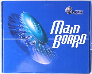
EPoX 4SDA+ (SiS 645) Mainboard
|

The blue box hides a pre-production sample, though it is of high quality
and has a rich set of accessories.
Accessories:
- Package: an ordinary design for this company;
- Documentation: a user manual in English;
- Cables: 1 ATA66/100, 1 ATA33 and 1 FDD;
- Bracket with two USB ports for the rear panel;
- CD with software including:
- drivers;
- system monitoring program;
- Boostek - for changing a FSB frequency from Windows;
- Adobe Acrobat Reader;
- Norton Ghost 6.03;
- PC-Cillin 2000.

The layout has some disadvantages: IDE and FDD connectors are placed
behind PCI slots (because of the IDE RAID controller), and
audio-ins are located in front of the 2nd and 3d PCI slots. There are also
two LEDs which monitor the POST procedure.
The feed circuits incorporate 6 capacitors of 3300 uF and 4 of 2200
uF.
There are the following controllers: AC'97 codec ALC201A from Avance
Logic (audio solution) - the chip supports SPDIF, but the respective connector
is lacking; IDE RAID controller supporting ATA 133 protocol
on the HPT372 from HighPoint.

There are no any non-unsoldered elements on the board.
Brief characteristics of the board: memory slots - 3 DDR SDRAM;
expansion slots - AGP/ 6 PCI; I/O ports - 2 COM/ LPT/ 2 PS/2/ 6 USB; dimensions
- 305x245 mm.
Adjustment can be carried out with:
| jumpers and switches |
Jumper to clear up CMOS |
 |
| Jumper to set a base processor frequency |
Auto, 100 and 133 MHz |
| Switches to set core voltage |
1.475 - 1.85 V, 0.025 V steps |
| Switches to set additional core voltage |
From +0.025 to +0.175 V in 0.025 V steps |
| Switches to set memory voltage |
2.5 - 3.2 V, 0.1 V step |
| Switches to set AGP bus voltage |
1.5 - 2.2 V, 0.1 V step |
| BIOS based on v6.00PG from Award |
Setup of memory timings |
+ |
CAS Latency, System Performance, DRAM Addr/Cmd Rate |
| Setup of memory frequency |
+ |
DDR200, DDR266, DDR333 |
| Setup of AGP bus |
+ |
 |
| Setup of PCI bus |
+ |
 |
| Changeable scaler of AGP and PCI buses |
- |
 |
| Manual assignment of interrupts |
+ |
 |
| Changeable FSB frequency |
+ |
In 1 MHz steps, 100 - 200 MHz |
| Changeable CPU multiplier |
+ |
x8 - x50 |
| Changeable core voltage |
+ |
1.4 - 1.85 V in 0.025 V steps |
| Changeable memory voltage |
+ |
From +0.1 to +0.7 V in 0.1 V steps |
| Changeable chipset voltage |
- |
 |
| Changeable AGP bus voltage |
+ |
From +0.1 to +0.7 V in 0.1 V steps |
This board from the overclocker-friendly manufacturer isn't very speedy
this time. However, it is much faster than many other today's competitors.
Besides, it was just a pre-production sample.
Test results:
Write a comment below. No registration needed!
|
|
 |
|
|
|


