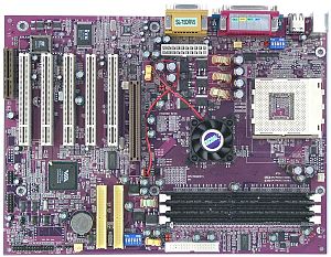
Soltek 75DRV5 (VIA KT333) Mainboard
|

The PCB is redesigned much as compared with the boards based on KT266
and KT266A chipsets, and one of the pleasant changes is standard connectors
for USB ports - the previous versions used special 15-pin connectors, and
the current one has a 9-pin connector. Besides, this is the first time
when Soltek paints its board purple.
Accessories:
- Package of a standard design;
- Documentation: a user manual and a software guide in English;
- Cables: 1 ATA66/100 and 1 FDD;
- Additional thermistor;
- 2 CDs including:
- drivers;
- PDF manuals for different boards;
- several system monitoring programs;
- program for changing a FSB frequency from Windows;
- Adobe Acrobat Reader 5.0;
- Trend Micro PC-Cillin 2000;
- Farstone Virtual Drive 6.01;
- PowerQuest PartitionMagic 6.0;
- PowerQuest Drive Image 4.0.

The layout is not the best: audio-ins are in front of the PCI slots,
IDE connectors are behind them, and a power supply is between the socket
and the AGP slot. Some switches and jumpers can be difficult to reach when
the board is in the case. Almost all switches and jumpers have their functions
specified.
The 3-channel switching voltage regulator incorporates 4 capacitors
of 2200 uF and 3 of 1200 uF.
The following controllers are integrated: an audio one based on the
capabilities of the chipset and AC'97 VIA VT1611A codec. The ITE IT8705F
I/O controller allows installation of a connector for a smart-card reader.
Non-unsoldered connectors: none.
The board uses system monitoring supported by the ITE IT8705F chip.
Processor voltage (+/-3.3, +/-5 and +/-12 V), speed of 3 fans and
temperatures of the processor (a built-in sensor), the board (a built-in
sensor) and an external sensor can be controlled. There are 3 connectors
for adjustable connection of fans.
Brief characteristics of the board: memory slots - 3 DDR SDRAM;
expansion slots - AGP/ 5 PCI/ CNR; I/O ports - 2 COM/ LPT/ 2 PS/2/ 4 USB
1.1; dimensions - 305x225 mm.
Adjustment can be carried out with:
| jumpers and switches |
Jumper to clear up the CMOS |
 |
| Switches to change a CPU multiplier |
x5-x12.5 |
| Switches to change a FSB frequency |
100, 120, 133, 140, 150 and 166 MHz |
| Jumper to choose memory voltage |
2.5, 2.6 and 2.7 V |
| Jumpers to set voltage of the AGP
bus |
1.5, 1.6 and 1.7 V |
| Jumper to set the Power Lost Resume
mode |
Enabled/Disabled |
| BIOS based on v6.00PG from Award |
Setup of memory timings |
+ |
CAS Latency, Bank Interleave, Burst Length,
Queue Depth, Command Rate, System Performance |
| Setup of memory frequency |
+ |
by SPD, 133 MHz, 166 MHz |
| Setup of AGP bus |
+ |
 |
| Setup of PCI bus |
+ |
 |
| Changeable scaler of AGP and PCI buses |
- |
 |
| Manual assignment of interrupts |
+ |
 |
| Changeable FSB frequency |
+ |
In 1 MHz steps, 100-200 MHz |
| Changeable CPU multiplier |
+ |
x8-x24 |
| Changeable core voltage |
+ |
1.1-1.85V, in 0.025V steps |
| Changeable memory voltage |
- |
 |
| Changeable chipset voltage |
- |
 |
| Changeable AGP bus voltage |
- |
 |
We used the latest available version of the BIOS - T1.1.
In general, this board looks attractive for overclockers, it is just
lacking for some functions of switches in the BIOS.
Test results:
Write a comment below. No registration needed!
|
|
 |
|
|
|


