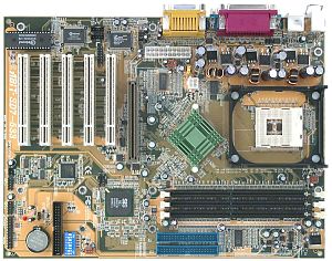
Abit SD7-533 (SiS 645) Mainboard
|

This board is one of the best among SiS 645 based models tested in our
lab - it offers good functions, rich settings and excellent speed characteristics.
Accessories:
- Package of a standard design;
- Documentation: a user manual in English;
- Cables: 1 ATA66/100 and 1 FDD;
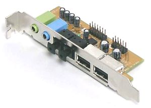
- Bracket with 2 USB ports, connectors for TosLink and audio adapter's central
and rear channels;
- CD including:
- drivers;
- Norton Antivirus 2002;
- WinDVD 2000 v.2.1;
- 3Deep;
- BuzzSoft SoftPostCard;
- BuzzSoft SoftCopier;
- BuzzSoft SoftCardManager;
- BuzzSoft SoftBulkEmail.

The layout is not very good: audio-ins are located in front of PCI slots,
an FDD connector is behind them, and power connectors are between the socket
and the AGP slot. Some connectors are unsoldered badly, though this is
a pre-production sample. Switches and jumpers are easy to reach even when
the board is in the case, but their functions are not shown.
The 3-channel switching voltage regulator incorporates 4 capacitors
of 3300 uF, 4 of 1200 uF and 2 of 1800 uF.
The following controllers are integrated: an audio one based on the
C-Media CMI8738/PCI-6ch-MX chip.

Non-unsoldered connectors: none.
The board uses system monitoring supported by the Winbond W83697HF chip.
Processor voltage (+/-3.3, +/-5 and +/-12 V), speed of 2 fans and temperatures
of the processor (a built-in sensor) and the board can be controlled. There
are 2 adjustable and 1 unadjustable connectors for fans.
Brief characteristics of the board: memory slots - 3 DDR SDRAM;
expansion slots - AGP/ 5 PCI; I/O ports - 2 COM/ LPT/ 2 PS/2/ 6 USB 1.1;
dimensions - 305x230 mm.
Adjustment can be carried out with:
| jumpers and switches |
Jumper to clear up the CMOS |
 |
| BIOS based on v6.00PG from Award |
Setup of memory timings |
+ |
CAS Latency, RAS to CAS Delay, RAS Precharge,
Write Recovery Time |
| Setup of memory frequency |
+ |
 |
| Setup of AGP bus |
+ |
 |
| Setup of PCI bus |
- |
 |
| Changeable scaler of AGP and PCI buses |
+ |
FSB/MEM/AGP/PCI: 2/2/2/1, 10/15/6/3, 16/20/10/5,
15/24/10/5, 3/6/2/1, 48/80/30/15, 12/20/10/5, 8/8/6/3, 3/3/2/1,
3/4/2/1, 4/3/2/1, 4/4/2/1, 4/5/2/1 |
| Manual assignment of interrupts |
+ |
 |
| Changeable FSB frequency |
+ |
in 1 MHz steps, 100-165 MHz |
| Changeable CPU multiplier |
+ |
x8-x24 |
| Changeable core voltage |
+ |
1.1-2.2 V, up to 1.85 V in 0.025V steps, higher
- in 0.05V |
| Changeable memory voltage |
- |
 |
| Changeable chipset voltage |
- |
 |
| Changeable AGP bus voltage |
- |
 |
We used the latest available version of the BIOS - 7R.
I wish it was possible to change voltage of the memory, the chipset
and the AGP bus, but the board still has a lot of changeable parameters.
This is the only sample we have tested which allows setting the memory
frequency of 200 MHz without lifting that of other buses - processor, AGP
and PCI ones.
Test results:
Write a comment below. No registration needed!
|
|
 |
|
|
|

