NV17M: Go Far, Go Fast... Lost NOW!!!
|
Here it is, the Next Generation Mobile GPU, or
just NV17M, a new child of NVIDIA. The most of the aspects which
will be addressed today will concern not only the mobile solution
but also a budget one, NV17, which is to be announced a bit later.
Let me outline the current situation around the NV17M.
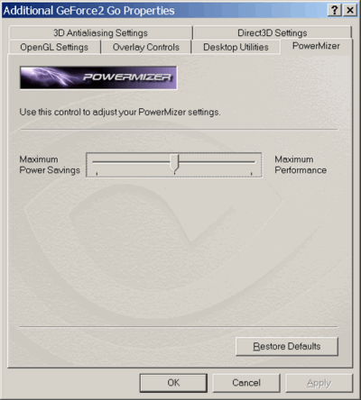
- The new firmware technology Powermizer is designed to provide
more effective power consumption, as well as a possibility to
adjust a performance/power ratio of the graphics accelerator integrated
into a notebook. If you manually decrease a limit of the peak
chip's performance (available settings are some 1/2 and 1/3 of
the maximum value) the power consumed by the chip at the highest
load (e.g. in a game) will be almost halved. Here is how the new
tab looks like in the drivers:

Besides, the chip is able to decrease the frequency dynamically,
depending on the instantaneous value of the load (even down to
16 MHz in the Idle mode of Windows) and maintain the respective
supply voltage. Consumed power is linearly dependent on the frequency
and is proportional to the voltage squared, that is why it is
quite a baffling problem to make a chip being able to change both
values. At last, the chip can "freeze" for a short time
if there is "nothing to do" (the frequency is equal
to 0 and the power consumed is also almost zero).
- MPEG2 (DVD) Hardware Decoding. It is a good response to the
hardware IDCT conversion which has been living in ATI products
for a long time already. The NV17M implements IDCT and IQ (Inverse
Quantization -ATI can't fulfill this initial stage of decoding)
on the hardware level, as well as Motion Compensation and Color
Space Conversion. It is stated that the utilization of the processor
decoding a DVD video stream is 3 times lower now (from 45% to
15%), which is a large commitment to the overall power consumption
of a notebook.
- I'm glad there is an integrated TV-Out controller and other
outputs: 1*CRT + 1*DVI + 1*TFT controller for an LCD display of
a notebook.
- The NV17M combines the technologies of two chip generations
(!):
- 0.13 fab process - NV25
- MSAA (including Qincunx) - NV20/25
- ZCompress and ZCull HSR - NV20/NV25
- Hardware DVD reproduction - NV25
- T&L Second Generation - NV11/NV15 (it is exactly GeForce
2 *, as vertex shaders, probably, consume too much).
- 250 MHz clock speed and a normal 128bit DDR memory bus are
promised.
- 3 versions of the chips are expected:
- Usual version with an external memory bus (128 and 64bit
memory bus optionally)
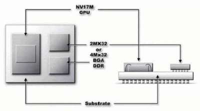
- MAP (Mobile AGP Package) - with 16 or 32 MBytes integrated
DDR (64bit bus). A die of the accelerator's core and two memory
dies are mounted on the chip case, over the microboard.

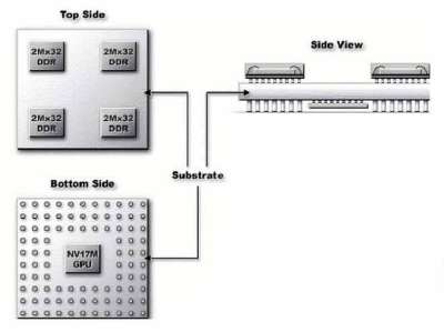
- MAP version with 64 MBytes integrated DDR (128bit bus).
A die of the accelerator's core (below the microboard) and
four memory dies are mounted on the chip case.

- The declared memory bandwidth is 8 GBytes/s, and the effective
one is 9.6 GB/s. It means that there are no compromises as in
the NV11: we have a normal 128bit DDR bus and a normal internal
memory controller on the chip.
- The most interesting thing is a chip configuration. Reportedly,
it has some 4 Gigapixel effective AA fillrate; i.e. taking into
account 4X MSAA the maximum fillrate is 1 Gigapixel, hence 4 pixel
pipelines. But now the site shows different figures (and I consider
them more credible) - 500 Mpixel/s of a true maximum fillrate.
It means that like in the NV11 we have two pixel pipelines with
two texture modules on each. Will it be possible to accumulate
the results for combination of 4 textures per clock (like in the
NV20)? We will do our best to find out it.
An interesting marketing argument is that a powerful, T&L
equipped chip is able to save energy when implementing the tasks
which earlier made the central processor consume a great deal
of power. This is a work on the main errors of the GeForce 2 Go.
The performance gain is impressing: a 1.5 or even double lead
on the closest competitor from ATI (M7) in the majority of tests.
I have an ocean of guesses about parameters of the future non-mobile
NV17 family. And now there is no information concerning real effectiveness
of energy-saving technologies and typical operating time of notebooks
working in intensive 3D applications. We shall see what we shall
see...
Write a comment below. No registration needed!
|
|
 |
|
|
|
