 |
||
|
||
| ||
For 80% of participants the Computex display, held in the beginning of June in the capital of Taiwan, is domestic and is located in the complex situated on the street full of central offices and factories of leaders of IT industry. According to practically all top mainboard manufacturers, for Taiwanese companies a success exactly in their own motherland is a guarantee of a successful business. By the way, almost the whole local motherboard market is shared by ASUS and Gigabyte, which compete against MSI, AOpen and ECS. As a result, at Computex everyone is eager to introduce as many new products and perspective technologies as possible, as well as to work out additional marketing steps in order to gain authority among distributors and journalists. One of such steps is excursions to factories where mainboards, CD drives, notebooks and other things are produced. Of course, I was mainly interested in the former ones. Unfortunately, among a wide range of excursions I happened to visit only two of them, conducted at AOpen and ASUS factories. But invitations came also from Gigabyte, ABIT, EpoX and Acorp. Gigabyte, however, invited us at the same time as ASUS. By the way, while the plants of Gigabyte do not differ from those of competitors, their office building is one of the posh and fashionable ones in Taibei. I missed the excursion to the ABIT plant by sleeping. Excursions of EPOX and Acorp were "neglected" due to lack of time. Organizations of excursions differ - ASUS and Gigabyte drive people to their plants in buses and forbid to make photos, while AOpen and EPOX offer exclusive tours. AOpen even allows making photos. So, the AOpen's factory. Not so long ago ACER Group, which AOpen belongs to, has purchased technological park Aspire, for building new factories. The factory of AOpen for manufacturing mainboards was first to raise at Aspire Park - apart from it there is only a university. The factory looks appallingly... 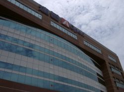 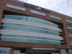 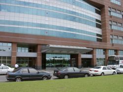 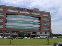 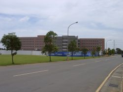 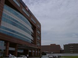 Inside it looks like an hotel. The visitors start to think that at such a beautiful factory bad products can't be produced. On the right of the administrator's stand there are glass cases with products manufactured here.   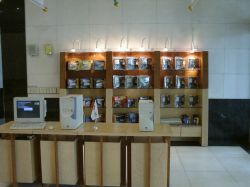 Before the excursion let's take a glance at the certificates. 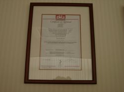 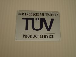 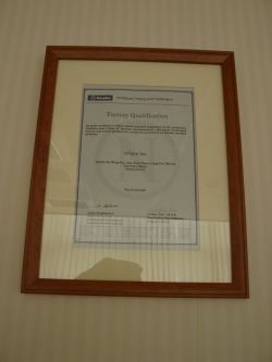 They were proudly demonstrated by our guide Mr. Ted Tsai - he is Director of MB Engeneering Department. 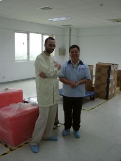 On the other hand, he is a person who is the most competent in all details of the process of production. The PCB Manufacturing Center is located on the 5/6th floors. Near the elevator there is a board with a detailed layout. 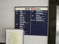 In the cellar you can find a restaurant, at the first floor there are an administrative department and two procurement departments (it seems that one purchases components for mainboard manufacturing, and the other - for optical devices), a customs registration department and a finished-products storage area. The second floor is taken by offices of managers and a service department. The third floor deals with production: optical devices and Barebone -half-ready systems are assembled there. The fourth floor is intended for storage of components for mainboards and optical devices. And the fifth and the sixth floors are our destination. Look at the hall and the elevator: 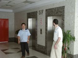 In the hall you can find a basic scheme - the scheme of production of mainboards meant for inexperienced excursionists. 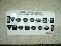 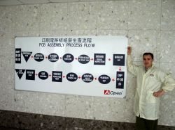 The manufacturing process consists of two basic stages - SMT (Surface Mounting) and a additional manual mounting (DIP). Each stage takes its own floor. Before entering the workshop each visitor must put on a special antistatic overall and socks worn above boots. In the workshops ideal cleanness is maintained. Visitors and workers have different antistatic overalls: yellow and blue ones. At last, a metallic door is opened. 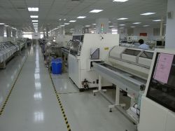 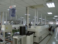 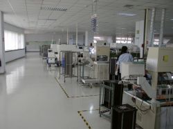 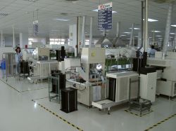 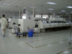 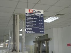 Here you can look at the surface mounting workshop. The boards installed in the beginning of each of four production lines contain a list of equipment used at all stages of the SMT process. From the storage area on the fourth floor the workers deliver virgin PCBs, which, by the way, are not produced by mainboard manufacturers. There are around five companies in Taiwan which produce printed-circuit boards by request of MB manufacturers. The printed-circuit boards are delivered in special carts. Then they are put into a production line and delivered to the conveyer. 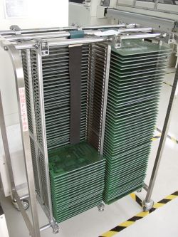 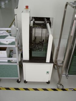 Now let's look at the difference between SMT and DIP stages. The surface mounting means soldering of components on the same side of the board where components are attached to, and the DIP stage means soldering of them on a back side. For the SMT stage it is necessary to cover a board with special soldering paste, which components are glued to. After that everything is put in ovens - the process is called Reflow. The surface mounting lines are supplied by Japanese companies such as Panasonic, FUJI and Yamaha. AOpen uses the latest equipment from Panasonic, ASUS has it from FUJI, and EPOX - from Yamaha. One SMT line costs some $1.5 million, a service life is about 10 years. The equipment breaks and get damaged quite rarely. The Solder Paste Printer is the first machine in a conveyer chain. 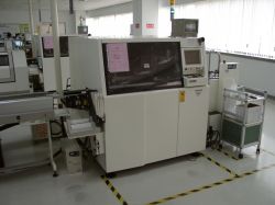 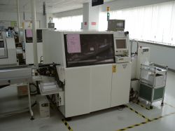 A special template is put on a board, which then is smudged with gray viscous paste. The a template is removed, and paste is left only on those places which are intended for soldering. 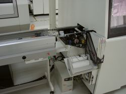 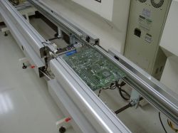 After that a board comes to the mounters for installation of components. Complex surface mounting is implemented with the help of four machines, and a simpler one is carried out with three ones. The workshop has totally 14 surface mounting machines on 4 production lines, the first two lines have three machines, and the other two have four ones. Simple components, from resistors to small chips, are installed by High Speed Mounters. More complex, like south and north bridges, are attached by Multi Function Mounters. High Speed Mounters can work with internal cassettes where small parts are located, and with external tapes which contain large parts such as chips. 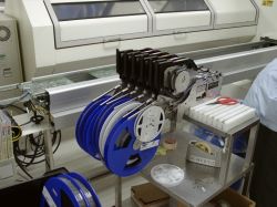 The first mounter sets the smallest parts. The speed of installation is up to 10 pieces per second. Installation of each component is controlled with a special camera. 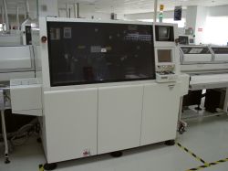 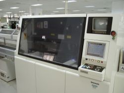 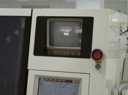 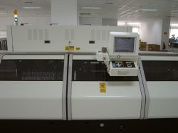 The second and the third mounters install parts which are soldered in the tapes. 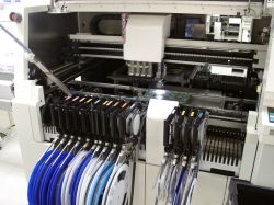 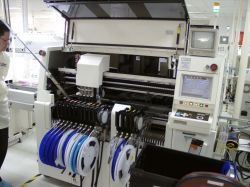 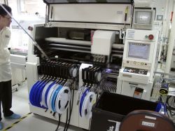 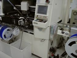 When a tape ends the process stops, a green indicator goes off and a yellow one goes on. A sound signal calls an operator who replaces empty tapes. 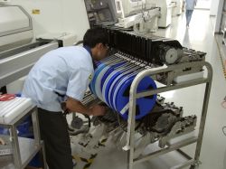 The last come the largest chips installed with Multi Function Mounters. Since large chips differ in size and package, they needs special holders. First of all, a mounter chooses a right holder and then takes it and installs on a board. On the photo you can see a process of installation of a north bridge. 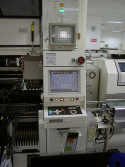 After installation of all parts boards proceed into the Reflow Oven. Different parts of the board heat differently from 30 to 230 degrees C. The temperature map is displayed on a large monitor. A graph of heating and temperature modes for all boards are shown on a separate illustration. 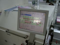 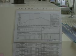 The warmed-up boards need cooling. For this purpose there are special fans on the output of the ovens. 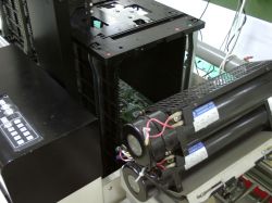 After that the boards are tested. The preliminary test consists of two stages - In Circuit Test and Visual Inspection. The first stage is conducted with a machine which reminds me a press. The board is put on a table and covered with a plate with conductors, which abridges definite contact groups. If not all signals pass, a monitor displays an error, and the board is sent for debugging. But the test may turn to be successful even the board lacks for some element. That is why after that a visual inspection is carried out to control the presence of all components. For each model there is a template made of green plastic which covers the whole board and has cuts in those places where components are to be installed. 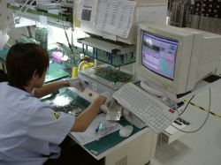 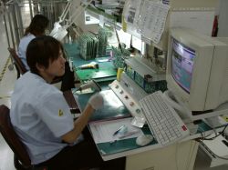 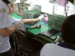 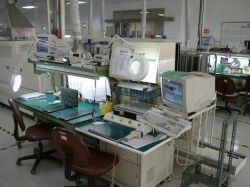 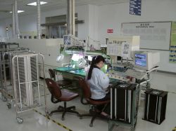 The boards are put into carts and delivered to the second floor by elevator, where missing elements are to be installed manually. In the second workshop there are much more people, while in the first one each SMT line is controlled by only several workers including testers. Well, the most part of the personnel deal with installation of elements which are soldered onto a back side. It is very difficult to automatize this part of work. Capacitors, sockets and other connectors differ severely in size and physical characteristics. In principle, it is not a problem to create such machines, but it is much more beneficial to keep people for it - 15-20 workers will install all components with not less efficiency than the most perfect machines. Installation of components in holes means their ideal adjustment in seats, that is why the accuracy of positioning of components by people doesn't yield to precision of machines. 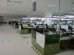 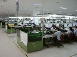 Then boards are put on a conveyor and start moving slowly. Operators who sit on the right and on the left install several components each according to the instruction in front of them. By the way, all operators are women. It seems that women are more assiduous and patient: 8 hours a day they have to put green and purple cylinders on their places. Moreover, no other nation in the world is able to work as a live conveyor so much time as Taiwanese and Chinese. It is interesting that AOpen prefers Chinese girls, while, for example, ASUS takes mostly women from Philippines. But everybody agrees that women from the continental China are the most diligent. By the way, New Chinese factories have newer SMT equipment than those used nowadays in Taiwan. 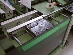 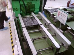 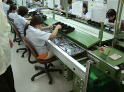 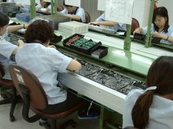 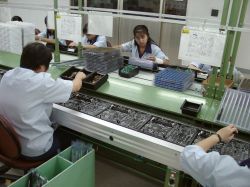 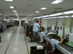 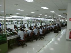 The last operator checks all the components before a board proceeds to Wave Soldering. What is wave soldering? Many think that such a soldering process is implemented with a water wave. 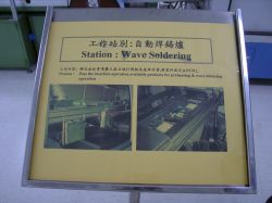 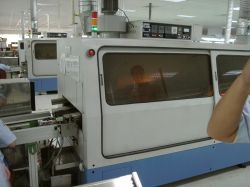 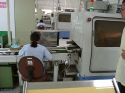 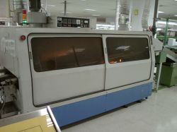 A the ASUS's factory an older oven from FUJI has a transparent glass through which you can clearly see a wave, but we were forbidden to shoot it. So, a board that comes into the oven, first of all, warms up in order not to become deformed at a sharp temperature change, and then a lower part of the board goes over a thin wave of molten tin at 190 temperature C. All metallic parts become soldered. Tin doesn't stick to the PCB, that is why the board remains clean. The boards are cooled with a ventilating system, which is much more serious that that of the Reflow Oven. 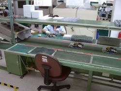 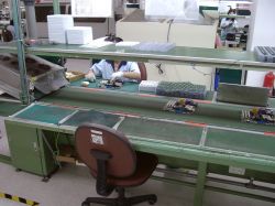 Well, now a board is nearly finished. At the last stage called Touch Up, workers attach heat sinks on chipsets and checks whether all elements are well soldered and whether there are no remains of tin on the back side. Each operator has a soldering iron to remove tin. 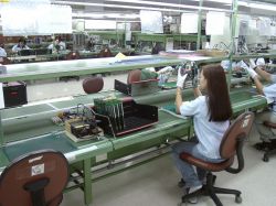 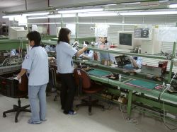 Now it is the right time for final tests. The Function Test includes two stages. 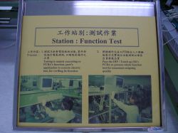 The first one called I/O Function Test is the simplest and means installation of a processor, memory modules, a video card, connection of a keyboard and installation of a POST card. The test culls the boards which didn't pass the POST. 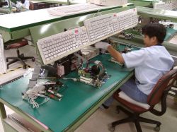 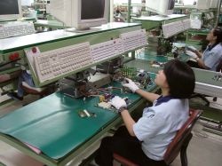 The second stage called Aging Test is much longer - around 30 minutes, that is why each operator serves not two-three stands, but around 20. 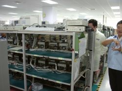 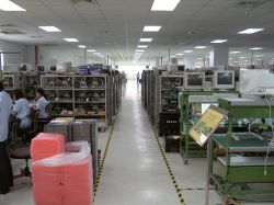 At this stage workers connect a hard disc, a CD-ROM drive and a mouse, and then an image of a disc from a CD is transferred on an HDD. After that an operating system boots, and Winstone runs three times. If a board passes the tests it ships to packaging. By the way, AOpen is proud of these half an hour tests - all other manufacturers only boots Windows, and its successful booting serves a signal for packaging of the board. But it is not an end - before packaging a board is switched on once more, and only if started successfully it gets an individual number and a sticker with a bar-code. 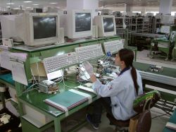 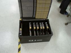 Then boards, as well as the other components of a package, are delivered from storage areas on black trays. 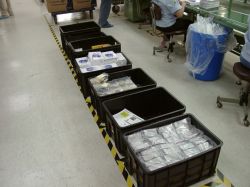 This one is a packaging line. Unfolded packages and antistatic packets are laying in piles. 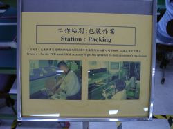 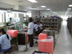 The boards are packed in big cardboard boxes (10 pcs per box) which are delivered to the finished-products storage area. 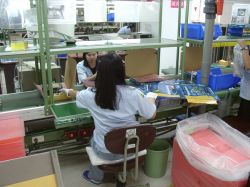 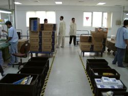 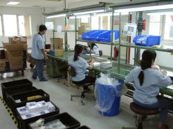 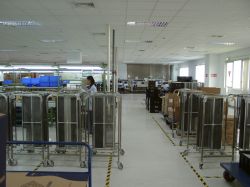 Unfortunately, ASUS doesn't permit to shoot their factories, you can look at them only from outside. This one, with policemen, is a factory for manufacturing mainboards and video cards: 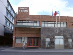 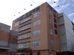 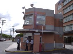 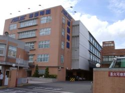 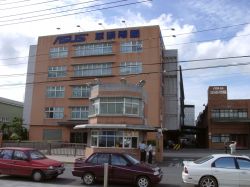 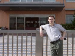 This one produces optical devices and notebooks. 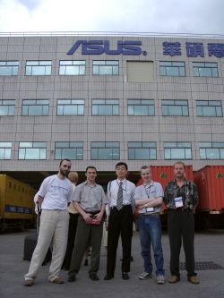 When I visited the factories, they produced only OEM equipment for SONY - one of them manufactured mainboards for SONY PC, the other dealt with notebooks on which you will see VAIO. We express our thanks to:
Write a comment below. No registration needed!
|
Platform · Video · Multimedia · Mobile · Other || About us & Privacy policy · Twitter · Facebook Copyright © Byrds Research & Publishing, Ltd., 1997–2011. All rights reserved. |