 |
||
|
||
| ||
|
||
|
||
| ||
1. Instruction Level ParallelismMost of modern processors have a similar architecture which is speculative superscalar outoforder execution design; it concerns both RISC and X86. The approach implies that several functional units (FU) operate simultaneously in the processor and exploit instructions from a special buffer, if possible, where they proceed to after decoding. The advantage is that parallelization doesn't depend on a programmer (at least, in higher-level languages) and it's unnecessary to apply special algorithms and language constructions used for development of programs for computers with several processors. One can think that by increasing the number of FUs it's possible to achieve a very high degree of ILP (Instruction Level Parallelism, ILP). It's true to some degree. But the superscalar architecture has a lot of limitations which grow as the number of execution units increases. For example:
According to some estimates, to double the ILP level regarding modern superscalar processors it's necessary to provide about 128 GPRs and 8 ALUs + 8 loadstore units. It will probably be realized in future IA-64 chips, but even now the same speed-up can be achieved for a vast deal of applications by simpler ways. 2. Thread Level ParallelismVarious TLP (Thread Level Parallelism) technologies are one of the ways to boost up performance of superscalar processors. Processors which use this approach exploit several instruction flows simultaneously. Multithread programs benefit from the TLP - for them it makes sense to use the already existent parallelism in programs optimized for multiprocessor systems. Usage of some SMT variation (Simultaneous multithreading), for example HMT (Hardware Multi-Threading) from Intel, is a temporary solution. This technology is able to provide a more effective FU load and optimize the memory access of existent superscalar architectures, and flows are divided by the same processor's FUs. It's estimated that the performance gain is 10-30% for different programs on the Xeon processors (this is Pentium 4, in fact). Another example of realization of the SMT is a server processor of the Power PC IBM RS64 IV family which is a predecessor of the POWER4 in the pSeries 6000 (RS/6000) and iSeries 400 (AS/400) systems. [1] On the whole, the SMT is logical and simple in realization improvement of modern processors. The Chip MultiProcessing (CMP) is a more radical approach which implies that several processor cores are located on one die. At present this technology has reached the level when it's possible to put two complex superscalar processors and enough amount of cache on one chip. We thus get an SMP system, and as the cores are located on the same die it makes possible to increase much a data rate between the processors in comparison to using any external buses, commutators etc. It is interesting that in the early 90s Intel considered to develop such processor - the 786 chip codenamed Micro-2000 was to have 4 cores, additional 2 vector processors and to work at 250 MHz. Just compare with the Pentium 4 :). The POWER4 consists of 2 identical processor cores which implement PowerPC AS instruction set, the die measures about 400 mm2, it's based on the 0.18 micron copper SOI IBM CMOS 8S2 technology with 7 metallization layers, works at 1.1 and 1.3 GHz, and is the fastest microprocessor for today. There is also a POWER4's variation with one processor on the die. However, HP and SUN are also going to release CMP processors soon which will be based on the 0.13 micron fab process. It's possible that AMD will follow this way as well. 3. IBM POWER4 - introductionThis processor is meant for the maximum performance, for hi-end server and supercomputer market, designed for 32-processor SMP systems. Development of high-performance communication means for processors and memory was given much attention to. The POWER4 has a high fault-tolerance: critical fails do not make the system hang; instead, interrupts are generated and then processed by the system. The POWER4 was developed for an efficient operation of commercial (server) and scientific and technical applications. Note that earlier the IBM Power/Power PC processors were divided into server and scientific ones - POWER and RS64. The POWER4 suits a wide range of hi-end applications and uses all topical performance boosting ways (within the PowerPC instruction set). We won't find there truncated caches and lacking FUs. The chip's design looks unusual; later we will see why the frequency of the POWER4 jumped from 600 MHz of the RS64 IV to 1.3 GHz. 4. POWER4 dieThe POWER4 houses 2 processors each having an L1 cache for data and instructions. The die has a single L2 cache of 1450 KBytes controlled by 3 separate controllers connected to the cores via a CIU (Core Interface Unit). The controllers work independently and can process 32 bytes per clock. Each processor uses two separate 256-bit buses to connect the CIU for data fetching and data loading, as well as a separate 64-bit bus to save the results; the L2 cache has a bandwidth of 100 GBytes/s. The L2 cache's system looks well balanced and very powerful. Each processor has a special unit to support noncachable operations (Noncacheable Unit). The L3 controller and the memory's one are located on die as well. For connection with the L3 cache working at 1/3 of the processor's speed and with the memory there are two 128-bit buses operating at 1/3 of the processor's frequency. The throughput of the memory interface is about 11 GBytes/s. Data flows coming from the memory and L2 and L3 caches and the buses of the chips are controlled by the Fabric Controller:  The 32-bit GX Bus running at 1/3 of the processor's frequency is used to connect to the I/O subsystem (e.g., by the PCI bridge) and a commutator in case of multiple nodes which contain POWER4 chips for creating clusters. 5. SMP capabilities4 POWER4 chips can be packed into one module forming a 8-processor SMP. The POWER4 chips are connected via 4 128-bit buses used on one module; they operate at 1/2 of the processor's speed. They are realized as 6 unidirectional buses, three in one direction and three in the other, and their total throughput is about 35 GBytes/s.  Take a look at the 4-chip module: (such silicon pieces can be found, for example, in a 32-processor pSeries 690 Model 681 server).  IBM focuses on the fact that a central commutator used for connection of the 4 POWER4 chips is replaced with multiple rapid independent point-to-point buses. AMD is going to use this approach in its future systems on the Hammer processor. For creation of multimodule systems it's possible to use up to 4 modules which allow for 16-processor SMP system or, taking into account 2 processors on each POWER4 chip, for a 32-processor one. Two unidirectional 64-bit buses are used to connect other modules; they form a ring topology:  The POWER4 is not meant for SMP systems with the number of processors more than 32. 6. POWER4 coreThe POWER4 core is much different from its predecessors as it uses the approach applied in modern X86, - transformation of PowerPC instructions into internal and group formation. So, a separate POWER4 processor is a superscalar core with speculative out-of-order execution. There are 8 pipeline execution units in all - two identical floating-point pipelines each able to implement addition and subtraction at a clock, i.e. up to 4 floating point operations at a clock, two loadstore units, two integer-valued execution devices, a branch execution unit a logical execution unit. Operations of division and square-rooting for floating-point figures are not pipelined and can worsen the POWER4's performance much. Look at the pipeline of the POWER4: 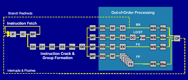 The integer-valued pipeline has 17 stages! It contrasts to the previous IBM chips with their 5-stage pipeline. Let's dwell on some interesting peculiarities of the POWER4 core. The L1 cache is capable of delivering to the front part of the pipeline up to 8 instructions per clock according to the address given by the IFAR register the contents of which is determined by the branch prediction unit. Then instructions are decoded, cracked and groups are formed. In order to minimize the logic necessary to track a large number of in flight instructions, groups of instructions are formed. A group contains up to five internal instructions referred to as IOPs. In the decode stages the instructions are placed sequentially in a group, the oldest instruction is placed in slot 0, the next oldest one in slot 1, and so on. Slot 4 is reserved for branch instructions only. To reach a high clock speed the POWER4 cracks PowerPC instructions into a greater number of simpler instructions which then combine into groups and are executed. If an instruction is split into 2 instructions we consider that cracking. If an instruction is split into more than 2 IOPs then we term this a millicoded instruction. Register renaming is widely used in the POWER4, in particular, 32 GPRs are renamed into 80 internal registers, 32 FPRs into 72 registers. It's clear that many once attractive peculiarities of the PowerPC are out-dated, and the processor gets new units for transformation of instructions into a form more convenient for execution. A processor with such a long pipeline needs an effective branch prediction algorithm. For dynamic prediction the POWER4 uses 2 algorithm versions and an additional table which tracks the most effective algorithm for a certain branch instruction. The dynamic prediction can be overriden by a special bit in the branch instruction. By the way, such feature appeared also in the X86 line with the Pentium 4. There are 3 buffer types to speed up translation of virtual addresses into physical ones - a translation lookaside buffer (TLB) for 1024 entries, a segment look-aside buffer (SLB) - a completely associative cache for 64 entries, and an effective-to-real address table (ERAT). The ERAT is divided into two tables - for data and for instructions for 128 elements. More detailed information on the POWER4 architecture and optimization of programs can be found in the IBM's guide [3]. 7. Caches and memoryThe following table shows key data on the memory subsystem:
Latency of the L1 cache is 4 cycles (for Pentium 4 - 2 cycles, for Athlon - 4). The L2 cache uses the MESI protocol for coherence support, and its average latency is 12 cycles (for Pentium 4 - 18, for Athlon - 20). But sometimes its latency can rise up to 20 cycles. Controllers of the L3 cache and of the memory, as well as the tag directory are integrated into the chip, and the cache consists of two 16 MBytes eDRAM chips mounted on a separate module which is divided into 8 banks of 2 MBytes. An important feature of the L3 cache is a capability to combine separate caches of POWER4 chips up to 4 (128 MBytes) which allows using address interleaving to speed up the access. The L3 cache is connected to the memory controller via two bidirectional 64-bit buses which operate at 1/3 of the processor's speed. The memory (200 MHz DDR SDRAM) is connected to the controller via two ports each consisting of 4 32-bit buses working at 400 MHz. So, the memory throughput when the two ports are used is a bit over 11 GBytes/s (the respective parameter of the Intel McKinley which is not released yet is 6.4 GBytes/s). Each chip has its own bus to the L3 cache and memory. The POWER4 has a hardware prefetch unit which loads data into the L1 cache from the whole memory hierarchy, and there are instructions which allow controlling this process on a software level. 8. Happy End
The Alpha is fading, and the POWER4 has no more competitors as far as processor power is concerned. The new Pentium 4 looks impressive in comparison to pale Itanium and PA-8700, despite announcements of aging IA-32 and advanced IA-64 technologies. Will the McKinley with its more powerful IA-64 be able to stand against the POWER4 at least in computational tests? Will SMT be integrated into personal POWER4 processors? What kind of CMP chips are other companies going to unveil? Literature
Write a comment below. No registration needed!
|
Platform · Video · Multimedia · Mobile · Other || About us & Privacy policy · Twitter · Facebook Copyright © Byrds Research & Publishing, Ltd., 1997–2011. All rights reserved. |


