 |
||
|
||
| ||
|
||
|
||
| ||
Manufacture, technology, equipment
 So, it's the end of the first quarter of 2002, and semiconductor market researching companies are eager to report the results for this year and share the corrected forecast. The January bottom line of semiconductor manufacturers at least assure in the normal operation start and show that downturn has finished. According to Semiconductor Industry Association (SIA), world chip sales made $10.01 billion in January, levelling with the December 2001 results in total, but differing throughout regions. So, the sales grew in North America and slightly in Asia, but dropped in Japan and Europe. However, it's still far behind the year-ago market activities: worldwide semiconductor sales volume dropped by 35.5% comparing to January 2001 and made $15.48 billion. The market is mainly afloat because of shipments of chips for mobiles, DVD devices, and digital cameras. iSuppli published the Top 30 of the best semiconductor vendors of 2001.
It shows only three companies out of ten last-year leaders and 6 out of the Top 30 '2000 saved their places. The DRAM manufacturers suffered most: Toshiba, Samsung, Micron Technology. However, it's not that bad. Foe example, the European STMicro jumped from the 6th to the 2nd place, outrunning NEC, Samsung, TI, and Toshiba. AMD entered the top 10 from the 16th place, and NVIDIA not only jumped 21 places up, but also showed the considerable sales volume growth of 81.2%! In general, according to iSuppli, only 27 of 172 companies were profitable last year. Only one segment of semiconductor industry out of 49 - 32-bit microcontroller manufacture - tended to grow. And only 5 out of 50 companies with over $500 million income experienced the growth. It seems to be like a fire if not the plague. Except for CeBIT 2002, being the most important industry event, March brought the SPIE conference important enough for semiconductor equipment manufacturers. The general issue was the development of the next generation EUV (Extreme Ultraviolet) lithographic equipment along with 157 nm equipment implementation. The very high expenses for the next-generation lithography (NGL) 0.07-micron tools development became the most troublesome issue for developers. These tools will cost very much because of such expenses. According to the market forecasts announced on SPIE, EUV tools, appearing on the market in 2007, will cost about $40 million and even more. No need to say what will happen in 5 years, when the prospective value of 157 nm scanners, expected in the nearest couple of years, reaches $25 million. Just compare: the most expensive 193 nm tools now cost $10-20 million per set. Joint efforts of several companies seem to be a logical step for cutting down R&D expenses. We've known of just two joint EUV projects before - the North American Extreme Ultraviolet LLC and Japanese ASET. SPIE brought the announcement of another group, European this time. The new EUV consortium lead by ASML Holding NV was named MEDEA+ and united French, German, and Dutch companies and research centers: Leti labs, Sagem, Sopra, Xenocs, and Carl Zeiss. Besides, there's the huge amount of smaller alliances and unions, appeared on the wave of the last economic downturn. Here's the short list of the most important events of SPIE:
But let's return to the current affairs. In the end of the month Applied Materials announced the new all-in-one eMax EnTek Centura tool for dielectric etch, photoresist strip, and barrier removal. eMax EnTek Centura can handle 200 mm and 300 mm plates and work in 100 nm and lower production lines.
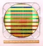
 The system extends dual-damascene copper processing by shortening plate processing stages, and is optimized for a wide range of etching damascene materials from Applied, including low-k films. The company applied its new sensor iRM (integrated rate monitor) technology for increasing the precision of trench etch depth control. On CeBIT 2002 Intel announced the smallest SRAM cell having just 1 sq.micron in size. It's the construct of the fully functional SRAM chip, produced according to Intel's 0.09-micron technology. This confirms company plans for mass implementation of the new technology in 2003. Intel stresses that all products of this technology will be manufactured exclusively on 300 mm silicon plates. The new 52 Mbit SRAM chips were created by the company on the experimental 300 mm D1C fab in Hillsborough, Oregon, with the combination of 193 and 248 nm lithographic equipment. In a couple of weeks Nikon Precision announced its 193 and 248 nm scanners and i-line steppers were used to create the industry first 90 nm chips, not announcing the chip manufacturer. Both companies refused to name their partners. Tower Semiconductor announced the successful launch of the pilot line for 200 mm silicon plates production with usage of 0.18-micron technical process, licensed from Toshiba, on the new Fab 2 in Migdal Ha'emek, Israel. The fab is expected to produce up to 33 thousands of 0.18-micron and smaller 8" plates per month at the moment of full capacity launch. Fab 2 is expected to work at the planned production capacity closer to the end of 2002. March brought several strategic alliances for 0.09-micron technical process implementation, this issue being the most pressing for most industry leaders. Many companies are going to launch such manufacture already in 2003. Philips, STMicroelectronics, and TSMC announced the unification of their developments in the field of 90 nm CMOS technical process implementation and the continuation of joint R&D efforts. The agreement will also cover the development and implementation of 0.065-micron and smaller technical processes. However they specified that the cooperation would be limited to joint R&D works, companies aren't planning to build joint production capacities. Another group for researching new semiconductor production technologies was created under the aegis of the Japanese government. It includes five leading chip manufacturers: NEC, Toshiba, Fujitsu, Hitachi, and Mitsubishi. The alliance will have been finishing forming the joint enterprise by the June 2002. It's interesting to mark the government's role in this venture: with ?500 million capital investments (about $3.8 million) of five companies, the Japanese Ministry of Economics, Commerce, and Industry is going to invest about ?31.5 billion (about $240 million). In March HyperTransport Consortium was traditionally updated. Its new full members include: Hewlett-Packard, Hifn, NEC Electronics, NurLogic Design, Phoenix Technologies, SandCraft, Schlumberger Semiconductor Solutions, Seaway Networks, and GDA Technologies. In March AMD opened the center for HyperTransport server technologies and solutions development to support and advance its venture. The so-called "Boston" center in Boxborough, Mass., USA, will become the subdivision of AMD Computation Products Group. According official establishment comments of AMD, Boston Design Center was created to develop specific HyperTransport applied solutions. ProcessorsTwo recent months were a fountain of Intel's technology: research and production initiatives, new platforms and architectures bubble one after each other. Announcements, made at IDF Spring 2002 in the end of February, smoothly lead to new solution demos at CeBIT 2002. During this period the company succeeded to release 0.13-micron chips on 300 mm plates, announce the 100-millionth box processor, present the next generation of XScale processor architecture for integrated, mobile and network solutions, begin the deliveries of the new generation server chips, etc. But let's be orderly. The presentation of the working 0.09-micron 4 GHz desktop Pentium 4 at IDF became the demonstration of technological growth. It's still long to wait for Prescott CPU mass production, it's expected from the second half-year of 2003, but Intel's technical potential was demonstrated enough. Prescott CPUs, already named "Hammer killers" by journalists, will also be the first chip for desktop PCs with Hyper-Threading support. Prescott chips are also expected to work with 533 MHz FSB (based on 133 MHz) and 667 MHz FSB (based on 166 MHz), core voltage will make about 1.2V, crystal size - 81 sq.mm. According to preliminary data Prescott chips might reach 5-6 GHz at Intel's transition to 90 nm P1262 technical process with the new high-k dielectrics (instead of SiO2). Japanese sources seriously discuss the possibility of Mobile Prescott due to expected low energy consumption. Besides, 0.09-micron technical process will also be used to produce 32-bit Nocona CPUs to replace Prestonia chips as well as 64-bit Montecito CPUs, the successors of Deerfield and Madison expected in 2004. Both Nocona è Montecito will be intended for dual- and more CPU servers, at that market will see their single versions instead of specific ones for every sector like now. 32-bit server Intel Xeon Pentium 4 (Prestonia) with Netburst architecture, Hyper-Threading support and 400 MHz FSB are already delivered to Intel's OEM partners. In the middle of 2002 the company will begin mass-delivering 0.18-micron 64-bit McKinley CPUs; and the summer will bring the first samples of new generation 0.13-micron 64-bit Deerfield and Madison. Their difference is that Deerfield is an economical 64-bit CPU for dual-processor configurations with energy consumption of 70-80W; for example, McKinley will dissipate about 130W. Madison is a high-end 64-bit chip with 3-6 MBytes of L2 cache, intended for the most performance solutions. Mass deliveries of both CPUs will begin in 2003. Getting closer to the current spring, let's remember that Intel presented the first 0.13-micron 1.7 GHz and 1.6 GHz mobile Pentium 4-M with 512 KBytes of L2 cache, 400 MHz FSB. The main difference of the new mobile CPU from stationary system CPUs is the advanced energy consumption control tools, prolonging battery life, such as Enhanced Intel SpeedStep technology, providing auto-switching between maximum performance and energy saving modes depending on CPU load; Deeper Sleep idle mode in which the processor consume only 1V, and power consumption drops to 0.2W and lower (at that keeping application data); improved Intel Mobile Voltage Positioning (IMVP) technology, that dynamically adjusts CPU supply voltage depending on its load and thus decreases the calculated heat emission intensity. 1.8 GHz Pentium 4-M is expected in the second quarter of 2002; 1.33 GHz mobile Celeron - in the third quarter.
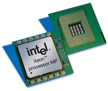 Intel released new 32-bit Xeon MP or Foster MP based on Pentium 4 core for the high-end server sector. Chips feature 1.4 GHz, 1.5 GHz, and 1.6 GHz clock rates; they are intended for 4-, 6-, and 8-processor servers. Xeon MP support Hyper-Threading Technology, have three levels of integrated cache, including up to 1 MBytes of L3 cache, 256 KBytes of L2 cache, and 8 KBytes of L1 cache. Intel released 0.13-micron 800 MHz Pentium III-S Tualatin for economical dual-processor blade-servers. Chips are intended for ServerWorks's LE3 chipset systems, consuming not more than 11.2W each. The mobile market was updated with 0.18-micron Xscale CPUs based on the RISC core with the ARM architecture - PXA250 and PXA210. PXA250 is for mobile PC market, featuring 200 MHz, 300 MHz, and 400 MHz clock rates; due to Intel Media Processing Technology it doesn't require an additional DS processor for multimedia applications. PXA210 line with about 133-200 MHz clock rates is intended for basic level pocket PCs and mobiles.
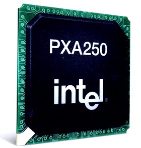 Both CPUs have 64 KBytes of integrated cache; integrated memory, LCD, Bluetooth, IrDA, USB 1.1 controllers; MMC/SD, PCMCIA, CF card interfaces. According to the general plan, it must reduce the total energy consumption of systems, based on them. New XScale products will be available in the middle of 2002. CPUs are intended for systems, based on Microsoft Windows CE.Net, Windows Pocket PC 2002. PalmOS, SymbianOS, and different Linux versions for integrated systems. Along with new chips announces, Intel continues to cut down CPU lines. The company actively gets rid of models with obsolete constructs and low clock rates, freeing production lines for modern chips. 0.18-micron 1.5, 1.6, 1.7, 1.8, 1.9, and 2 GHz Socket 423 Pentium 4 (PGA423) CPUs are taken out of production. 1.5 and 2 GHz Socket 478 (mPGA478) Pentium 4, 1.0 GHz Socket 370 Pentium III, 1.5, 1.7, and 2.0 GHz Intel Xeon (MPGA) along with the whole family of Pentium III-M and Mobile Celeron were cancelled as well.  However AMD did it best not to allow the spring to become Intel's gala performance. First, at the height of Intel Developer Forum, the company sparkled the working samples of its x86-64 Hammer processors. 0.13-micron SOI (Silicon on Insulator) ClawHammer was demonstrated under 64-bit Linux and 32-bit Microsoft Windows. The CPU was installed to the 4-layer SOLO 2 reference board, based on AMD-8000 chipset (AMD-8151 north bridge. AMD-8111 south bridge), with two DIMM sockets for PC1600/2100/2700 DDR SDRAM. The demo system had PC2700 memory. This ClawHammer configuration seems to feature only the single-channel mode with peak bandwidth of 2.7 GBytes/s and 2 x 2 GBytes Unbuffered, i.e. up to 4 GBytes, maximum memory size.
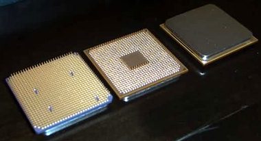 More performance SledgeHammer CPU will power systems, using dual-channel PC2700 (DDR333) mode, allowing to achieve peak bandwidth of 5.4 GBytes/s. It's worth mentioning that a server dual-processor ClawHammer version is being prepared for the release - the so-called ClawHammer-DP. However it's HyperTransport architecture will differ from the PC version. The pin amount will be the same, but the organization will differ: 8 bit x 2 vs. 16 bit x 1 of the desktop ClawHammer. ClawHammer and SledgeHammer will feature Socket 754 and Socket 940 respectively. CPUs have PGA case and heat sink like that of Pentium 4, sized 40 x 40 mm. However, it's still a long wait for mass samples of these chips: AMD is going to deliver the first ClawHammer family chips only in the end of 2002. AMD presented not many real processors. They were the three Athlon chips, announced prior to CeBIT 2002: desktop Athlon XP 2100+ (1.733 GHz), server and workstation Athlon MP 2000+ (1.67 GHz), mobile Athlon 4 1600+ for notebooks (1.4 GHz). All of them are produced at Fab 30, Dresden according to the 0.18-micron technical process. Despite AMD executives' statement, made at Hannover exhibition that the first 0.13-micron Thoroughbred chips would appear before the end of March, this hasn't happened. They've appeared neither for sale, nor as official announcements. The public still has to be satisfied with chips' photos, showed at AMD's stand at the exhibition. Still, according to informed yet unofficial sources, not desktop Athlon XP, but mobile Athlon 4 will be the first Thoroughbred chips. The information about the purchase of Alchemy Semiconductor and AMD's entry to the integrated 32-bti RISC MIPS microchips manufacturers has finally proven to be true. It took AMD just $50 million to pay Alchemy's shareholders and creditors. The company has become the owner of the rather successful low-voltage MIPS32 chips series, and also received the previously signed partnerships with Microsoft, Monta Vista, Philips Semiconductor, Epson and other leading market players. Besides Alchemy purchase, AMD, following its plan for developing mobile Internet gadgets, announced the creation of commercial Personal Connectivity Solutions subdivision. MIPS, that had automatically become the licensed partner of AMD, has already announced the development of cooperation in the field of its RISC processor architecture application. VIA Technologies announced the release of mobile processors to market, having presented the new µFCPGA Mobile C3 low-voltage CPUs, featuring clock rates up to 933 MHz, at CeBIT 2002.
 At the core supply voltage of 1.35V, Mobile C3 dissipates about 6W and is intended for notebooks, tablet PCs, Web consoles and other mobile devices. Processors are made according to 0.13-micron technical process; they have 128 KBytes of L1 cache, 64 KBytes of L2 cache; they work with 100/133 MHz FSB and support MMX and 3DNow! instruction sets.
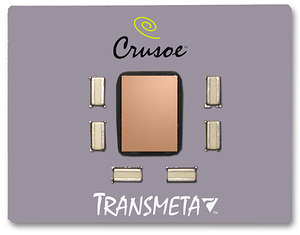 It seems Transmeta has at last mastered the release its Crusoe TM5800, making it without any fanfares. Release delays resulted in $23 million expenses, reported for the 4th quarter of 2001. But even this was not the most unpleasant thing for the company. According to analysts, Transmeta has missed the opportunity to enter the server market and lost potential partners in this sector: NEC, Toshiba, and RLX Technologies. These losses are rumoured not to be the last for company: Sharp decided to break the partnership with Transmeta. Now Japanese companies are going to use Intel's processors for their ultra-light notebooks. Only Sony and Fujitsu remain the true partners of the company. Motherboards and chipsetsMarch has been started by Intel, announcing the release of mobile chipsets with DDR support for Pentium 4-M - i845MP and i845MZ. i845MP chipset is intended for external AGP 4x graphics, 400 MHz system bus, up to 1 GBytes of DDR266 SDRAM memory, up to 6 USB ports, 100Base-TX, Ultra ATA/100, ACPI 2.0, etc. i845MP-based notebooks have already been announced by numerous manufacturers. In some time Intel will present its i845MZ chipset for integrated graphics without AGP support, optimized for inexpensive systems. Despite the announcements of Pentium 4 motherboards on i845G, i845GL, i845E chipsets, and their wide demonstration at CeBIT 2002, Intel is not planning to release them until May, according to the present information. So, let's postpone the discussion of these novelties to the next month, and talk of more topical things.
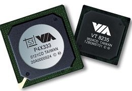 VIA used CeBIT 2002 to announce and demonstrate its new Pentium 4 P4X333 chipset. Besides DDR333 support, P4X333, as compared to P4X266, supports 533 MHz FSB, AGP 8x, USB 2.0 and UDMA 133 interfaces, and features the updated version of V-Link bus between chipset bridges with up to 533 MBytes/s bandwidth. Elitegroup's L4VXA was the first motherboard demonstrated on P4X333. When Intel announces its i845G, i845GL, and i845E closer to May, VIA is going to announce P4X600 version supporting 533 MHz FSB, AGP 8x, and 128-bit DDR266/333; and also AthlonXP KT400 chipset supporting 200/266 MHz FSB, AGP 8x, and DDR333/400 memory. The first trustworthy information about K8HTB chipset for AMD Hammer processors is expected about the same time. Besides, the company is going to begin deliveries of the new VIA VT8235 south bridge supporting V-Link 8x, dual-channel ATA133 IDE interface, 6 USB 2.0 ports, MII interface, Home PNA, 10/100 LAN and 6-channel AC97. The next south bridge version after VT8235 will be equipped with the dual-channel Serial ATA interface and will support wireless 802.11b protocol. VIA's striving for equipping motherboards, based on its chipsets, with the complete interface set was reflected in the peripheral chip line presented in March:
However, participating in the development of the standard PC architecture, VIA actively promotes its alternative - the economic Eden platform based on the combination of a processor without additional cooling and integrated Apollo PLE133 / ProSavage PN133T chipsets, plus VT8231 south bridge and Mini-ITX form-factor. Company's exposition at CeBIT 2002 included working prototypes of VIA Eden Embedded System Platform devices: an infostation, a TV console, a tablet PC, and a Web console from VIA's partners: Nexcom, Advantech, AAEON, ECS, and Microstar. Now VIA Eden is a proven fact, as products of the Total Connectivity platform are already used in serial solutions, for example, in iBuddie and iNote systems from ECS, HiServer blade servers, and OCTALTV multimedia consoles from Nexcom. Mini-ITX system boards have already interested such manufacturers, as MSI, AAEON, Unicorn, Commate, Axus, Netcom, Plexuscom, and Nexcom. VIA's immediate plan is to extend the platform with the VIA Eden Video Platform fully supporting MPEG2, "picture-in-picture" (PiP) mode, etc. The prospective development plan also contains the VIA Eden Server Platform VE3000 series and Multimedia Platform VE4000. 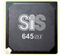 In the very beginning of the month SiS announced the release of Pentium 4 SiS645DX chipset, being the updated version of SiS645 supporting 533 MHz FSB along with usual 400 MHz. SiS645DX supports DDR333/DDR266/PC133 (up to 3 GBytes) memory, AGP 4x/2x bus. It features the well-known SiS961 south bridge, supporting 5.1-channel audio (AC'97 v2.2), 10/100 MBytes Ethernet and Home PNA2.0, ATA 133/100/66/33 IDE interfaces, up to 6 PCI slots and up to 6 USB 1.1 ports. Besides, SiS announced the long-awaited SiS962 south bridge, featuring integrated support of IEEE1394A and USB 2.0 interfaces (up to 6 USB 2.0 ports), and also the capability of working with MuTIOL bus (Multi Threaded I/O Link) with up to 1.2 GBytes/s bandwidth. 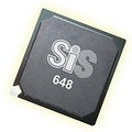 The company presented the new Pentium 4 SiS648/963 chipset with DDR400 support, 533 MHz FSB, and AGP 8x bus at CeBIT 2002. SiS963 south bridge adds to SiS962 MuTIOL 1 GBytes/s and HyperSoft ADSL support. The long-promised integrated ATi chipsets have debuted at last. Having been previously called A3/A4, presented as the RADEON IGP family. The series includes two north bridges for AMD - RADEON IGP 320 for desktop Athlon/Duron and RADEON IGP 320M for Athlon 4/Mobile Duron, and also three north bridges for Pentium 4 - RADEON IGP 330/RADEON IGP 340 (Pentium 4) and RADEON IGP 340M (Pentium 4-M). North bridges will be completed with IXP south bridges: IXP 200 and IXP 250, for desktop and mobile markets, respectively. They are equipped with 3Com integrated Ethernet controller, 6-port USB 2.0 interface, integrated 5.1-channel audio and PCI 2.3 slot support. Besides, IXP 250 supports extended remote control capabilities, Wake-on-LAN mode, etc.
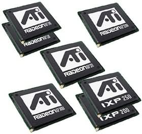 RADEON IGP family features 64-bit architecture and supports 266 MHz DDR memory interface, POWERPLAY, FLEXFIT, Fast Z-Clear, HYDRAVISION technologies, AGP 4x, and also has TV-out connection capability. Besides, IGP 340 supports 533 MHz FSB. CeBIT 2002 brought us only the prototype of ATi RADEON IGP 320 chipset, combined not with the original IXP 200 south bridge, but with the well known VIA 686B. The mass appearance of new chipsets is expected only in summer 2002. 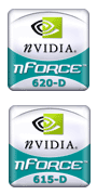 In March NVIDIA announced the release of the new generation of its AMD Athlon chipsets - integrated nForce 620-D and discrete nForce 615-D. Both support DDR333 memory. nForce 620-D and nForce 615-D samples have already been delivered to NVIDIA partners, and the ready motherboards are expected closer to the end of the second quarter of 2002. Besides, there were rumours that NVIDIA will at last begin to deliver the "light" version of nForce 420 in April - nForce 220 chipsets for inexpensive PCs, announced by NVIDIA last year. nForce 220 line includes two versions: nForce 220 with SDRAM support and nForce 220D with DDR266 support. It differs from nForce 420 chipsets by the absence of 128-bit memory controller. Nevertheless, chipsets feature many capabilities of the "senior" line: the same integrated graphics core, 5.1 Dolby digital, etc. The final price of nForce 220 boards will be about $90 per unit vs. the average $155 for nForce 420-D board. According to preliminary data, the next generation of NVIDIA chipsets, codenamed "nForce2", will be presented in June at Taiwanese Computex 2002 Taipei. Memory productsThe last month pushed the memory price issue to the top again. It's known that DRAM began to rise in price in November last year. Customers started to get used to the idea that purchasing memory is not a cheap thing; manufacturers gladly reported profitable quarters, when another downturn started. 128 Mbit SDRAM price dropped from $5 to $3.5 per unit for the month. Even Samsung, having almost foreseen the downturn due to the low activity of electronics customers at CeBIT 2002, and having decided not to rise DRAM contract prices at the end of March, still couldn't effect on this tendency. Further memory price changes are hard to predict, as there are too many hardly "predictable" factors. I'll just list some of them:
In other words, let's wait for major OEM customers to place numerous orders for memory products in the summer on the threshold of the Back-to-School season. DRAM market might change anyhow. The Jedex conference was the major event of this month. JEDEC members published the first details of DDR-II specifications. Unfortunately, JEDEC hasn't yet expressed a clear point about the standartization of DDR400 products, belonging the first generation of DDR, existing as samples from Samsung and Micron. It might be so that the market will move to DDR-II from the ratified DDR333 standard at once. Elpida, Hynix and Infineon decided not to produce 400 MHz DDR-I chips. Some companies' officials call DDR400 exotic, intended for specific offers, and do not see any sense in its standartization. JEDEC will prepare the final chip characteristics by June; and unit specifications will appear closer to September. The following DDR-II features are currently known:
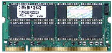
DDR-II product samples are expected closer to the end of 2002 / beginning of 2003, DDR-II becoming consumer in 2004. The conference also brought some words the "next next" generation of memory products - DDR-III, serious development beginning in 2004. Now we know that DDR-III will feed from not more than 1.5V with subsequent decrease to 1.2 V by 2006. JEDEC has also approved QDRII and DDRII SRAM memory architectures as the industry standards. According to the developer group - Cypress, IDT, Micron, NEC, and Samsung - the new JEDEC standards define the structure and pinout for every up to 288 Mbit QDRII and DDRII SRAM product. JEDEC standardized 165-pin fine-pitch ball-grid array (FBGA) case for future QDR memory products, providing 40% chip size decrease comparing to the traditional 209-pin BGA or 100-pin thin-quad flat-packs (TQFP) cases. QDRII and DDRII SRAM memory products support up to 333 MHz clock rates. They are intended for OC192 (10 Gbit/s) and OC768 (40 Gbit/s) products. Besides, the QDR Group might soon be updated with Hitachi, as the company has expressed the wish to join it. Transcend's low-profile 512 MBytes DDR SO-DIMM units in sTSOP package were the interesting product of the month.
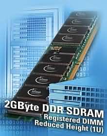
 They are only 1.25" in height, organized as 16 DDR 32M chips x 8 sTSOP. According to Transcend, they are twice smaller and much cheaper to produce than standard TSOP 64Mx8 chips. New 512 MBytes SO-DIMM units require 2.5V at up to 2.1 b/s performance (DDR266). They are 67.6 x 31.75 x 1 mm in size. Chips are purchased from Mitsubishi and other leading manufacturers. Infineon released engineering samples of 1 GBytes unbuffered dual-level DDR SDRAM DIMM units and demonstrated the fully functional 2 GBytes registered DDR SDRAM DIMM units included into Plumas/Prestonia platform.
 New 1 GBytes units, designed as 512 Mbit chips in TSOP II case, are intended for the high-end PC and workstation market; 2 GBytes units will be generally used in workstations and servers. 1 GBytes DIMM units are designed as eighteen 512
Mbit chips organized as 64M x 8. 2 GBytes DIMM units are designed
as thirty six 512 Mbit chips organized as 256M x 4. Both feature
the standard 184-pin DIMM design, 2.5V supply voltage. They'll be
released according to PC1600 and PC2100 standards.
Write a comment below. No registration needed!
|
Platform · Video · Multimedia · Mobile · Other || About us & Privacy policy · Twitter · Facebook Copyright © Byrds Research & Publishing, Ltd., 1997–2011. All rights reserved. | |||||||||||||||||||||||||||||||||||||||||||||||||||||||||||||||||||||||||||||||||||||||||||||||||||||||||||||||||||||||||||||||||||||||||||||||||||||||||||||||||||||||||||||||||||||||||||||||||||||||||||||||||||||||||||||||||||||||||


