 |
||
|
||
| ||
|
||
|
||
| ||
 Despite the Chinese New Year of the past month that has disbalanced the habitual work rhythm of some of the South Eastern companies for almost a week, February was rich enough with microelectronics news. Comparing the first quarter of 2002 to the same of the last year, it's nice to see the absence of decadent tendencies of factory closure, staff discharges and like. On the contrary despite the harsh year 2001, companies are mostly straining at the leash and making positive reports. EquipmentNow some statistics for the last year. Silicon plates shipment volumes of the year 2001 are indicative in this field. According to SEMI (Semiconductor Equipment and Materials Int.), plate shipments for chip manufacturers have made 25.4 billion sq.cm. In 2001 that is 29% less, comparing to 2000 (35.8 billion sq.cm.). Profits of this industry have made $5.2 billion that is 31% less then the $7.5 billion of 2000. Some more of the interesting statistics. Let's take a look at the Semiconductor Equipment Manufacturers Top Ten of the most unsuccessful year. According to VLSI Research, places are occupied by:
There are not so many famous news-flashers among these companies, moreover they are popular in other industries more. However, this list exactly enumerates power brokers of the semiconductor industry, whose "bakeries" and "batter" result in "pancakes" and "slapjacks" processors and other chips. The three leaders of this list Applied Materials, Tokyo Electron Limited, and Nikon have been remaining at their positions since 1992. Despite the most severe losses in the last year, they've managed to maintain stability. Lithographic equipment manufacturers suffered less than others. Their total losses were about 24% comparing to 2000, whereas test manufacturers lost 57.3% and other manufacturers lost 34.7%. ASML, the European lithographic equipment manufacturer, moved to the 5th place from the 14th in the year 2000, having purchased the North American Silicon Valley Group (SVG) in May 2001. Canon, Dainippon Screen, and Hitachi High-Technologies showed noticeable success, and raised their ratings to the 6th, 7th, and 9th places accordingly. Total sales volume of American companies reduced by 39% in average comparing to 2000. After ASML purchased SVG in 2001, there are only two companies, which work with optical equipment, remaining - Ultratech Stepper and Mulith Inc. However, not only the American companies lose their ratings. According to analysts, this also awaits European chip equipment manufacturers because of the continuing reduction of Japanese yen relative to USA dollar. The facts are not only the "spontaneous" circumstances like the recent tongue slip of the USA President George Bush, who occasionally confused yen devaluation and deflation, which resulted in the 15% fall of the Japanese currency (from 134 yen for $1 to 155 yen). According to Yahoo.Finance this currency has fallen by about 11% for the last three months already. Japanese companies are undoubtedly happy about this process as export volumes grow with yen falling. But this is really bad for Europe. According to Commerzbank experts, Dutch ASML will lose up to its sales in 2002. But it's not the worst: its Japanese rivals Nikon and Canon get additional benefits in the lithographic equipment manufacture sector as yen continue to fall. However, it seems that Nikon has already got ahead of ASML with at least one serious consumer. February brought news that Intel had at last chosen the 193 nm equipment vendor for the 0.09-micron technical process. According to the report of the BlackFin Research Partners investment company, Intel will purchase the first consignment of 193-micron argon-fluoride lithographic equipment from Nikon, thus paying less attention to the Dutch ASML Holding for now. It's known that another Japanese company Canon participates in these tools delivery tender, however BlackFin Research says that Nikon and ASML (or rather purchased SVG), Intel's traditional vendors, were the rivals this round. Intel, ASML and Nikon hasn't commented this yet, however BlackFin Research says that Intel has chosen Nikon NSJ system because of better optical co-ordination and elements layout. It's still early to speak of Intel's final decision, as analysts concur that company is anyway interested in deliveries of 193-micron equipment from more than one vendor, for instance due to different requirements of different factories. So Intel might use Canon's equipment along with that from Nikon and ASML in the future. Currently Intel uses 248-micron equipment from SVG to produce Pentium III and other 0.25 and 0.18-micron chips, and the DUV line of Nikon's NSJ tools is used for critical 0.13-micron layers for Pentium 4 production. Nikon i-line works at non-critical 0.35-micron layers production. All this is a traversed path for Intel. New 193-micron equipment, purchased from Nikon, is delivered to Fab D1C (Hillsboro, Oregon, USA), where Intel is assembling a pilot 0.09-micron line. Moreover, Nikon is getting ready to deliver the same tools for the Fab 11x in Alboukerke, New Mexico, USA, where Intel is going to launch production of 0.09-micron chips on 300 mm silicon plates in the very beginning of 2003.  Despite the exact dates of 193-micron lithography launch reported by some chip manufacturers, the technology itself is far from perfect, demanding serious revision. To speed up the 193 micron technology implementation, Belgian IMEC research centre in the middle of February announced the prolongation of the Industrial Affiliation Program (IIAP) for implementing 193 micron step-and-scan systems with the high numeric aperture (NA) into 100 micron and lower technological processes, which has started in 1999, until 2003. To continue the development IMEC purchased ASML's 193 micron PAS5500/1100 step-and-scan system with the maximal NA=0.75 combined with the Clean Track ACT8 resist coating line from Tokyo Electron. Now this complex is being assembled on pilot 8" IMEC line. The research is planned to March 2002.  The program is intended for research of 193-micron equipment with k1 between 0.35-0.3 for critical layers. 0.75 NA optics will help to reach and research 75-90 micron resolutions. To the moment of wide 193 micron lithographic equipment deliveries IIAP will result in the basic recommendation package for chip manufacturers, materials (resistors, ARC) and peripherals vendors. The program will further proceed to the next generation of 157-micron lithographic tools. To conduct quality control of 193 micron lithographic equipment and etching process at 0.10 micron and smaller chip manufacture, Applied Materials released the CD-SEM NanoSEM 3D, a computer-aided 3D control system, in February. 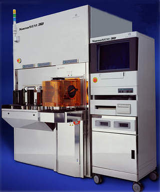 NanoSEM 3D uses electron bunches oriented at several directions at different angles, allowing to automatically monitor each plate in several planes. The critical-dimension scanning electron microscope (CD-SEM) allows the chip manufacturers to automatically view and measure upper and side chip elements in 3D. This adds quality to examining plates after skimming a photoresistive layer, to researching photoresistor shrinkage problems, improving etching process during work with the shallow trench isolation (STI), gates, and dual-damascene. As a whole the main current tendency is: despite industry has tightly advanced to wide implementation of 193 micron lithography for <0.1 micron technical processes, there's no common industry standard at all. Certainly, developing the whole manufacture cycle from the very beginning is rather costly, and not every chip manufacturer has enough funds and will to conduct independent developments.  Of course, companies having enough funds and suitable base implement 193-micron lithography independently. Scientific-research groups like IMEC are going to provide an alternative to this, offering a package of basic recommendations. There's also the third, more ambitious way. Some "practical" companies, for example TSMC, having advanced far in the 193-micron lithography implementation, offer their technologies as the industry base. In other words, it's the crossroads.  The Microlithography 2002 conference, organized by SPIE (Society of Photo-Optical Instrumentation Engineers), to take place on the 4-9 March in Santa Clara, CA, USA, will perhaps shed the light on this situation. The conference will let discuss all the questions regarding modern lithography, not only those about implementing 193 micron lithography for 0.09-0.07 technical processes.  At the same conference ASML together with European Carl Zeiss, Sagem and Xenocs is going to present its vision of modern lithography and show off the new EUV lithography developments. Companies call their "European" initiative Extatic (theEXTreme Ultraviolet Alpha Tool Integration Consortium). The purpose of the joint conference report is to show that Extatic can be used for <0.05 processes. Words "European initiative" sounds a bit contradictorily, as ASML has promised to become a "system integrator" for the American EUV LLC (AMD, IBM, Infineon, Intel, Micron, Motorola, US Energy Department labs). So, it's another strange paradox. SPIE is also expected to feature the report of Nikon that develops EPL lithography in parallel with IBM, and of Canon that develops EUV-equipment independently. SPIE might become the most important event of the first quarter of 2002 for semiconductor industry's equipment and materials manufacturers. TechnologiesSCT (Silicon Crystal Technologies) reported in February about getting two patents for the technology of growth, processing, and refinement of calcium fluoride, used for producing lens for 193 and 157 micron lithographic equipment (Continuous Crystal Plate Growth Apparatus). The low quality of currently grown calcium fluoride crystals results in only 3-5% yield for 157-micron optics requirements. The new method of calcium fluoride refinement allows to remove erbium (Er) and lutecium (Lu) impurities effectively and under control that allows to get rid of 157-micron fluorescence and achieve the more contrast picture. The purification from lead (Pb) additionally reduces 157-micron absorption.  Besides, SCT's method allows to control impurities and affect crystal's optical properties, including double refraction pattern. Researchers from Texas A&M University reported about the development of the plasma method of semiconductor crystal copper coating at room temperature. Copper conductors are usually coated with the damascene approach: channels are cut in the crystal's surface and filled with copper, followed by CMP. According to the new method, all copper layer is transformed to inactive copper halogenide (bromide or chloride), forming a porous layer on crystal's surface, which is dissolved by weak HCl liquid. Experts think this process to have better chances for success than the alternatives. The first figure shows the cross-section of copper plasma (400 micron), affected by molecular chlorine at 25 C temperature. 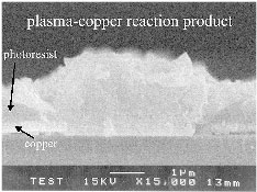 The process is unique because the oxidant is generated in plasma and substrate at constant ion bombardment. However, the copper layer can swell during HCl processing due to increasing volume at chlorine penetration of resulting layer's porous structure. Researchers compared this process with iron oxidation and rusting. The second figure shows the resulting sample. 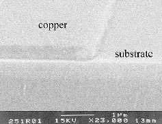 Other materials, affecting copper layer uniformity, were examined as well, and a simulator was created. Now researchers are creating micron copper conductors. Hitachi Research Centre and Massachusets Institute of Technology (MIT) announced the joint development of a low-voltage economical mobile chips production technology. The new technology bases on Hitachi's researches of substrate bias currents as well as on MIT's technology of supply voltage control. Currently they are getting ready for sample manufacture of 16-bit chip according to 0.14-micron CMOS technical process with 0.175 V supply voltage. This gets closer to the 0.1 V limit the theoretical CMOS chips limit for room temperature. Sequence Design announced the NanoCool initiative, aimed at facilitation of modern low-voltage 0.10 micron and smaller chip manufacture. The company intends to destroy fears, regarding power supply and noise problems at nanomicron semiconductors development. With tools from IP Wizard package for computer-aided modelling of semiconductor chip IP blocks power supply, which will become the program base, Sequence intends to speed up and facilitate the optimization of semiconductor chip power supply circuits. According to Sequence, IP Wizard package is already widely used by ARM.  Sequence's partners for NanoCool initiative are Silicon Metrics, Virtual Silicon, ARM and Toshiba. It's known that Silicon Metrics will work on improving noise characteristics, and Virtual Silicon will work on describing two-level cells. The company plans to present the Design Explorer tool for virtual power supply circuits synthesizing and heat emission analysys. Manufacture
 Toshiba's announcement has become one of the most interesting events of February: the company announced the release of the first experimental microprocessor using Diagonal Routing technology from Simplex Solutions. These are the first fruits of the famous X Architecture initiative. Toshiba's experts reported that diagonal routing of conductors considerably reduces delays as the total conductor length is reduced by 20%, and crystal square size by 10%, comparing to the traditional Manhattan Routing.  However, not all the layers of experimental processor were routed diagonally. Three of six use traditional x-y routing, two use diagonal routing, and the 6th has power supply and grounding buses. On the IDF Spring 2002 in the very end of February Intel announced the first consignment of processors using 0.13-micron technological process, produced on its 300 mm factory in Hillsboro, Oregon, USA. I guess everybody understands this as the beginning of mass production of chips on 300 mm plates. The sharp cost price reduction (hope due to the same or lower spoilage percent, as of 200 mm plates) will give Intel at least additional finance benefits. Plans for using Irish factories of the company were described in more detail at IDF Spring 2002. Despite Intel's management hasn't yet announced the final decision about prospects of constructing 0.09 micron 300 mm Fab24, it has become known that 0.13 micron equipment will be installed at Irish 0.18 micron 200 mm Fab 14. Intel has also clarified the production type: Fab 14 will produce XScale network processors, presented at the Forum: 10 GBit/s IXP2800, 2.5 GBit/s IXP2400, and IXP425 for xDSL, cable, and wireless office and home networks. By the way, IXP425 is the first processor developed completely at Intel's research center in Shannon. All processors will be produced according to 0.13-micron technical process. Texas Instruments announced plans of launching the new 0.09-micron technical process by the middle of 2003. According to company representatives, the main technological feature is that transistor gate width will make about 0,037 micron with the new CMOS. The new process will be used to produce chips for cellular phones, wireless devices, and UltraSparc processors, ordered by Sun Microsystems. TI's 0.09-micron technology combines 9-level copper connectors with organo-silicate glass (OSG) low-k (k=2.8) dielectric, allowing to increase areal density of 6T SRAM memory to 700 KBit/sq.mm. Besides, the new process will use plasma nitrided oxide (PNO) materials, developed by TI, for diode forming. Two new TI's factories in Dallas will be equipped with the new technology by the middle of 2003, but the mass production is planned to the end of 2003. Now, a little about China. North American DuPont Photomasks (DPI) announced the plans to build 0.18-micron photomasks production line in China, hoping to expand its existing factory. For this purpose the company purchased the newest laser template generation complex from Applied Materials. DuPont is going to begin licensing the equipment for its export from USA in the second quarter of this year, however the current export limit is 0.25 micron. Will DuPont overcome it? In case of success many companies might want to move 0.18-micron manufacture to China in the nearest two years. In other words, DuPont is to create a precedent, and we'll watch the process. In February VIA announced the start of its Canaan restructuring project, according to which, it's going to split its business into five departments: chipsets (including Platform Solutions Division, VPSD), processors, graphic chips, optical drive chips, and network solutions. It's still unknown what such restructuring might bring, but the idea is certainly noble. But what company doesn't dream of "Promised land"... In February it has become clear that the rumor about AMD's purchase of Alchemy Semiconductor, the manufacturer of 32-bit RISC processors with MIPS core, is true. For just $50 millions AMD purchased a titbit in the form of Alchemy, which after licensing MIPS32 architecture has succeeded to develop a serie of successful low-voltage processors and sign contracts with Microsoft, Monta Vista, Philips Semiconductor, Epson, and some other market leaders. Following its plan of active mobile Internet-devices development and mobile solutions release, AMD decided to create the Personal Connectivity Solutions department. MIPS, having automatically become AMD's partner, announced the intention of close cooperation for expanding the range of application of RISC architectures. UMC, being unprofitable in the last year together with the majority of brand semiconductor manufacturers, tries every marketing and technological trick possible. All this to return the profitability in the second quarter of 2002. Having reduced capital expenses to $800 million, comparing to the last year's $1.1 billion, the company has made some additional steps. UMC has added another partnership with Cirrus Logic to those with AMD and Infineon. According to the signed contract, UMC becomes the chip manufacturer for Cirrus Logic and the latter gets access to 0.10 micron and smaller digital-analog mixed chips manufacture technologies, being developed by UMC. Besides, the information that UMC is actively selling off-stream equipment to China, turned out to be true as well. The sale of 40% of its share in Trescenti joint venture enterprise with Hitachi, being the owner of a 300 mm silicon plate factory, became the most important February contract for UMC. According to the contract, Hitachi gets a brand new factory for undivided use, and UMC gets $70 million to reinvest to the continuation of its own Fab12A construction on Taiwan as well as to Singapore joint ventures with Infineon (UMCi) and AMD (AU Pte). Write a comment below. No registration needed!
|
Platform · Video · Multimedia · Mobile · Other || About us & Privacy policy · Twitter · Facebook Copyright © Byrds Research & Publishing, Ltd., 1997–2011. All rights reserved. | |||||||||||||||||||||||||||||||||||||||||||||||||||||||||||||||||||||||||||||||||||||||||||||||||||||||||||||||||


