 |
||
|
||
| ||
|
||
|
||
| ||
IntroductionIt's twice as hard to write about Intel's products. On the one hand, you can cause a tidal wave of indignation from admirers of this world famous corporation - it is no secret that processors, motherboards and other computer components with a proud inscription "Intel" on them are considered as those of infallible serviceability and crash safety for a long time already. And on the other hand, there are lots of monopoly production opponents, that don't like this company who read about its products with excessive captiousness and don't always interpret information in a positive way. Those delayed relations with Rambus now go to the "archive" (referenced to my article) - while the result is unobvious (not so good price / productivity ratio). High price is another disadvantage of processors in comparison with the competitors (those of AMD company first of all) and thereof weakening of Intel positions in lower and average computer market segments. Large investments in the communication devices market is a good strategic course, but it will bring dividends not at once, and it has distracted Intel from the processors market. The company wants to get higher in the ranks in the new year and therefore starts from the real blow to the competitors with the release of Pentium 4 processor at the end of the last year that has strengthened company's position in high and average computer systems price categories. (Here we still see the situation with Rambus - not so bad probably). The second blow was the release of new Celeron processor, which can conditionally be termed as a third generation processor (the second generation processors in these terms have Coppermine kernel). This CPU has at last long awated FSB 133 MHz "feature" - early Celerons worked at FSB equal to 66 MHz, while P-IIIs worked at FSB 100 MHz. This innovation will allow to lift a rod of perfomance of initial level systems, and that should bring results in the near future or Intel risks to lose clients. Certainly, the processor needs a chipset, which will allow to show all features it is capable of. The company presented a lot of chipsets for Celeron processors including old BX, office i810 (with integrated videoadapter and unavailability to change it for something else), and new i815E in two i815E and i815EP modifications - second lacks videoadapter and therefore board based on it will become a subject of our today's interest. So, under the order - The processorI shall remind Celeron's history briefly in order for you to understand what is so interesting in our experimental Celeron 800. Celeron processors were oriented by Intel on the market of below $1000 systems, and at the moment of the appearance they lacked L2 cache unlike their elder brothers - Pentium 2 processors. The unique advantage of cache absence was that almost all processors could be tweaked 1.5X and more comparing to the nominal of 266 and 300 MHz, but perfomance of even tweaked CPUs hardly exceeded Intel Pentium MMX's original (P-2s were in another price category). The time passed, and the company presented processors with new Mendocino kernel - they had the same S.E.P.P packing, but also had built-in L2 cache, and they worked on CPU's kernel frequency that was used by Intel for the first time since Pentium Pro and was a real step forward for home systems. The competitors from AMD, Cyrix and IDT were too feeble that time - they lost in speed of math coprocessor operation, and even new 3Dnow! instructions, applied in the K6-2 processor of AMD company could not oppose anything to this due to small number of applications that could use them. As the result the speed in new applications using "math" for 100%, was dramatically low - the most famous Unreal and Quake 2 3D-shooters had good graphics quality on cheap Celeron systems, and that was unavailable on competitor CPUs, which were used mostly for office computers. The "tweakability" of those processors has remained at a level of their predecessors - the majority of them worked perfectly on FSB 100 MHz. Then there was a still period, interrupted only by change of processor packing to PPGA, that has marked the return of the good old Socket-plugs scheme - this time it was Socket370. This solution was cheaper than slot solution (at the expense of refusal from $10 processor board, which was created to situate L2 cache closer to kernel). Then there was some silence again (frequencies were growing, but nothing new had occured) and then a novelty came true: Celeron, being at 533 MHz already, changed kernel to 0.18 micron Coppermine, packing to FCPGA, and gets new SSE instruction set. All this has appeared from the elder Pentium III brother, though differences were: the twice smaller cache (the half is simply turned off) and FSB 66 MHz has remained unchanged from first Celerons. Approximately the same time a first real competitor - Duron processor from AMD appears. It had no "heavy anchors" like slow FSB. And … Intel started to lose. AMD carried on aggressive price policy - cards for their new processor almost were not present (and so the price was high), the price for it appeared low, thereby cancelling difference in cost of motherboard+CPU couple, besides perfoamnce metrics appeared better due to 100 MHz bus. What did Intel do? Waited? No! They make a new Coppermine kernel with C0 stepping, which was to lift processor perfomance metrics at the expense of kernel heating decrease - and it concerned both Celerons and Pentiums III (which were made with new stepping since 700 MHz version) and allowed at those business standings, I mean rather old 0.18 micron technology, to save a perfomance parity with Athlon processors. In general, Celeron processor with FSB 100 MHz was awaited even earlier - in the beginning of '2000, but Intel may have decided to not make two mainstreams from one because then the low Pentium III models were to lose in price or leave the market for good, in other words it would result in profit losses. Taking into account, that there was not actual competition, the company could allow itself to have some rest. But those crafty guys from AMD released new Athlon on the ThunderBird kernel and then Duron and this changed Intel's life in a rough way. 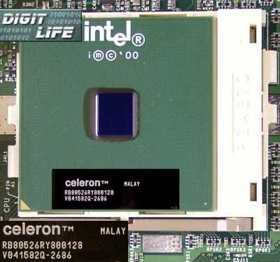 Such is the history of processors life. New Intel Celeron 800 MHz working on FSB 100 MHz is being released in the new millenium. The processor is made in already habitual FC-PGA packing, it differs from existing in decreased from 105sq.mm. down to 90sq.mm. chip size - a physical expression of the difference between new C0 stepping kernel and the old one. 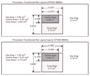 Nominal voltage systematically increases from the beginning of CPU releases - this time it makes 1.7V comparing to 1.5V of Celeron 533A. The kernel remained the same, but with frequency increase, it is necessary to raise power supply level to support operation stability. Processor specifications:
There are few changes in comparison with the previous Celeron processors, but increase of FSB from 66 MHz to 100 MHz is cardinal. Further we'll look at what it brought us. And now I want to proceed to the second part of the given browse - as I wrote earlier, Intel enters new year with new chipsets - i815E existing in two modifications - with built-in video on the basis of old i752 and without it - Intel recommends the last as the partner to Celeron processors. We got new Intel's D815EPEA in our laboratory, it is based on i815EP chipset and is more interesting product for system construction because there is no built-in graphics kernel, and it's cheaper than those boards on i815E basis. The boardI'll briefly observe chipset's features here, but you can find more detailed description in our browse of Asustek CUSL2-C board. 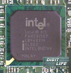 So what does Intel recommend us? Here are brief specifications of i815EP MCH north bridge:
As we see, Intel began to precisely divide two markets (or two segments), on which it orients different chipsets, processors etc., it strongly changes habitual concepts about mainstream chipsets. Intel realizes that there would hardly be more than 512 MBytes in the SOHO computers, or that this memory will need ECC error correction support, and the time it's a disadvantage, for competitors like VIA present more opportunities for the comparable price. As if to the south bridge - it the same 82801BA ICH2 for i815E and i815EP chipsets. Moreover there's "E" suffix in the chipset titles, and it tags what Input/Output Controller Hub (ICH) is there - in the very first chipset variant it was 82801AA, without ATA100 support, LAN controller, and 2 USB ports comparing to today's 4. The board itself, as all other Intel's boards, is one of the most stable devices on the market - Intel never makes other products, however sometimes to the detriment of perfomance. It is natural that the board is limited by chipset features - we don't expect anything else from Intel, it would be strange to see a manufacturer who is not holding on to his specifications:) Board specifications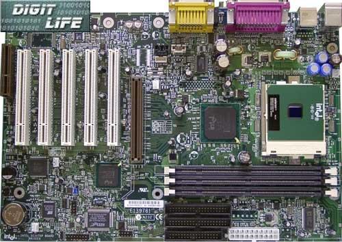
The board is among many released recently which became "victims of total unification" :) - it is made on PCB that is the same for several cards - for D815EEA for example (according the inscription on it), thereof there are unused DVI and videoadapter plugs, a place for Creative sound chip from, etc. The plug of the second serial port has remained on a front part of board due to standard - that is much more cheaper than to design new PCB and put it on a valid place. I was shocked by the presense of light diodes for POST procedure diagnostics on board - Intel was not engaged in anything similar before. 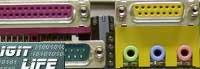 To tell the truth, I haven't seen Intel's boards for a long time (since SR440BX), but I had information that Intel has changed it's developers team - it has had a right effect. We have a very pleasant functionality convenient for the system constructors. In a complete set of accessories the back panel stub has appeared, as these light diodes are located between COM-port and Line-out. There are no such stubs in a usual set of ATX cases, naturally, there are no holes. 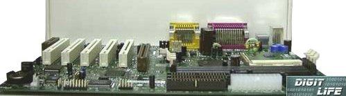 Besides, in standard for Intel's box (conservative as always) I have found IDE and IDE66 wide cables, floppy disk cable, very brief manual in English and one of the Asian languages, case sticker with a figure of board and jumper description with description of plug layout and a sticker with warning about incorrect battery usage. Also there was a small sheet concerning changes in the given manual (the manual was for D815EEA) and a CD with drivers, utilities for system monitoring, the most detailed board description in the Adobe Acrobat format and also one more innovation from Intel - there were Norton Antivirus 2001 and Norton Internet Security Family Edition 2001 software. And while first is well-known, I shall tell a couple of words about the second - it allows the user aware of the admin password to prohibit access on particular sites, to protect computer against unauthorized Internet access (Firewall) and to filter ad banners off. BIOS does not contain any "excessivities" - Intel considers that the board can set itself up better than user can do :) Intel Rapid BIOS Boot became a novelty (at least for me), it allows to reduce POST procedure time from 32s down to 6.2s (information is taken from the company website), though it is stipulated in documentation that not all HDDs can have time to pass the selfdiagnostics for this time. The "treatment" can be carried out by setting of HDD initialization delays in BIOS Setup. The POST time is a little bit longer than 6s, but nevertheless it is much faster than on earlier Intel's boards. Intel Express BIOS Update technology can be termed as a relative innovation - it is the possibility to update BIOS without OS rebooting (for Windows systems) that becomes actual with Windows ME, where there is no possibility to boot from the command prompt. The board is jumperless or should I say "jumper-one" as there's only one jumper for loading Setup in case of any incorrect BIOS adjustments or in case of password loss - in the same case a new BIOS menu appears - where it is possible to clear passwords and to set-up memory timings - I shall remind that you can't do it in the normal mode. Also (and this is standard for Intel) the third jumper position allows you to rewrite BIOS from diskette in case of some unplanned situation. Unfortunately, tweaking is not possible on this board (as well as on all other from Intel) - I shall remind that Intel not only releases motherboards, it is also a processor manufacturer, and it can't violate its own prohibitions. Due to all this we used Asus CUSL2-C motherboard, based on the same chipset, for tweaking. PerfomanceFirst of all we are interested in the new Celeron 800 MHz processor, and motherboard from Intel goes the second. It's not the first browse of Intel's motherboards, so the results mustn't differ greatly. CPU tweaking is the most interesting thing here, and comparison with Duron 800 MHz in particular. Test equipment:
And software:
A bit about tweaking: I haven't tried to select CPUs specially (it was impossible in case with Celeron), and the tests were conducted with just equipment available. Usual Intel's coolers were used in tests. We tried to make it a kind of "typical" variant. CPU voltage: Intel - 1.95 V, Duron - 1.85 V. Test results: 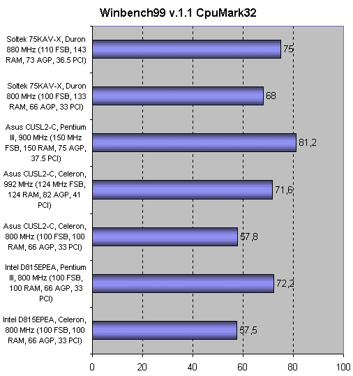 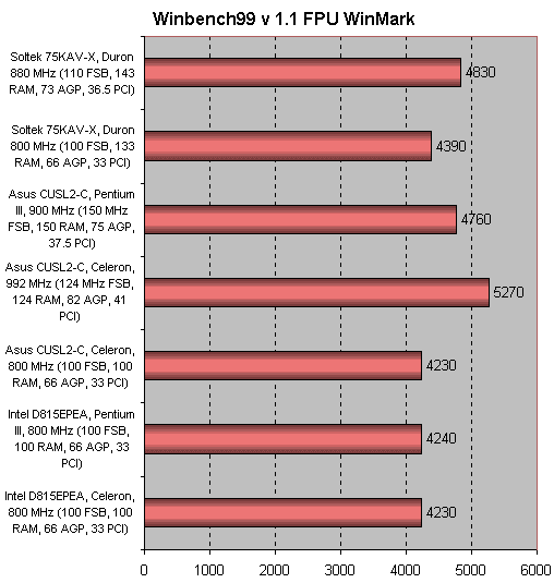 From Winbench test results we can see that coprocessor speed increases almost in a straght way with tweaking, and processor speed increase is less noticable. And even greater clock rate doesn't give that speed boost for Celeron. Probably it's due to a twice smaller cache in the first case and due to different cache organization in case with Duron, but anyway it could be expected. 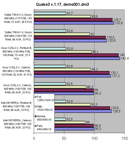 In this case we see that D815EPEA loses to Asustek - it was undoubted, though maybe it will be possible to "squeeze" something out of it as there are no new BIOSes now. Concerning the perfomance: Pentium III rules. Celeron does not make it even with a new system bus. Strange results in 1024X768X32 resolution I relate to a measuring error. In 1280X1024X32 resolution we see that everything rests on videocard perfomance, and all processors show equal results. 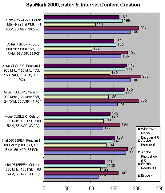 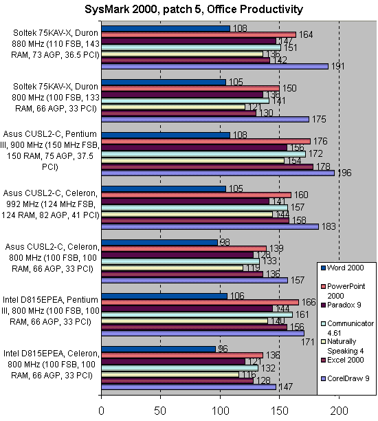 In common Pentium III has won the tests operating with actual applications (though Duron was ahead in some cases), Duron was the second - Celeron outruned it slightly in a tweaked mode, but on nominal frequency Duron took top. Optimization of some applications (like Adobe Photoshop or Windows Media Encoder) for Intel's SSE instructions showed up - unfortunately, 3DNow! instruction set has appeared more difficult to programmers, so they usually write for SSE. What's in total?The processor is good, but not as it might have been. Duron has better cache organization and a stronger coprocessor "curve" Celeron's innovation. Taking into account the price of about $170, while AMD Duron costs approximately $100 less - the new Intel's processor is a doubtful purchase, probably, it is necessary to wait for some lower prices for it. The board, though does not display outstanding results, is an excellent choice for speed undemanding users. It is no secret, that speed is frequently gained to the detriment of stability. Write a comment below. No registration needed!
|
Platform · Video · Multimedia · Mobile · Other || About us & Privacy policy · Twitter · Facebook Copyright © Byrds Research & Publishing, Ltd., 1997–2011. All rights reserved. |


