IBM Research Creates World's Smallest 3D Map
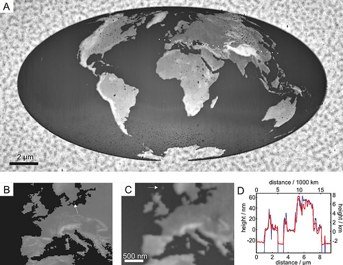
IBM scientists have created a 3D map of the earth so small that 1,000 of them could fit on one grain of salt (0.3mm). The scientists accomplished this through a new, breakthrough technique that uses a tiny, silicon tip with a sharp apex -- 100,000 times smaller than a sharpened pencil -- to create patterns and structures as small as 15 nanometers at greatly reduced cost and complexity. This patterning technique opens new prospects for developing nanosized objects in fields such as electronics, future chip technology, medicine, life sciences, and optoelectronics.
To demonstrate the technique's unique capability, the team created several 3D and 2D patterns, using different materials for each one as reported in the scientific journals Science and Advanced Materials:
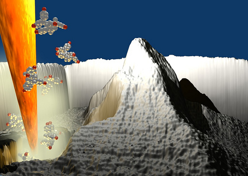
- A 25-nanometer-high 3D replica of the Matterhorn, a famous Alpine mountain that soars 4,478 m (14,692 ft) high, was created in molecular glass, representing a scale of 1:5 billion.
- Complete 3D map of the world measuring only 22 by 11 micrometers was "written" on a polymer. At this size, 1,000 world maps could fit on a grain of salt. In the relief, one thousand meters of altitude correspond to roughly eight nanometers. It is composed of 500,000 pixels, each measuring 20nm², and was created in only 2 minutes and 23 seconds.
- 2D nano-sized IBM logo was etched 400-nm-deep into silicon, demonstrating the viability of the technique for typical nanofabrication applications.
- 2D high-resolution 15-nm dense line patterning.
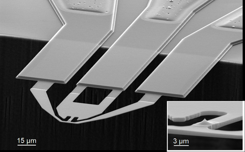
The core component of the new technique, which was developed by a team of IBM scientists, is a tiny, very sharp silicon tip measuring 500 nanometers in length and only a few nanometers at its apex.
The tip, similar to the kind used in atomic force microscopes, is attached to a bendable cantilever that controllably scans the surface of the substrate material with the accuracy of one nanometer. By applying heat and force, the nano-sized tip can remove substrate material based on predefined patterns, thus operating like a "nanomilling" machine with ultra-high precision.
Similar to using a milling machine, more material can be removed to create complex 3D structures with nanometer precision by modulating the force or by readdressing individual spots. To create the 3D replica of the Matterhorn, for example, 120 individual layers of material were successively removed from the molecular glass substrate.
The new IBM technique achieves resolutions as high as 15 nanometerswith a potential of going even smaller. Using existing methods such as e-beam lithography, it is becoming increasingly challenging to fabricate patterns at resolutions below 30 nanometers, where the technical limitations of that method are reached.
What's more, compared to expensive e-beam-lithography tools that require several processing steps and equipment that can easily fill a laboratory, the tool created by IBM scientistswhich can sit on a tabletoppromises improved and extended capabilities at very high resolutions, but at one-fifth to one tenth of the cost and with far less complexity.
Yet another advantage of the nanotip-based technique is the ability to assess the pattern directly by using the same tip to create an image of the written structures, as the IBM scientists demonstrated in their experiments.
Potential applications range from the fast prototyping of nano-sized devices for future computer chips to the production of well defined micron-sized optical elements like aspheric lenses and lens-arrays for optoelectronics and on-chip optical communication.
In the two publications, the scientists describe their novel 3D-nanopatterning methodology for two very distinct and promising types of substrate materials: a polymer called polyphthalaldehyde and a molecular glass similar to substrate materials used in conventional nanofabrication techniques, so-called resists. Identifying these two materials was a key factor for the breakthrough performance and reliability of the technique.
In their search for suitable and efficient substrate materials, the scientists concentrated on organic materials that could be used as resists, thereby following the same philosophy as used for today's semiconductor technology, which is important for further integration.
The molecular glass that was used in the Matterhorn experiment consists of snow-flake-like molecules, measuring about one nanometer and having an almost spherical shape. At a tip temperature above 330 degrees C (626 degrees F), the hydrogen bonds that hold the molecules together break, allowing the molecular parts to become mobile and to escape from the surface. A particular strength of the material is that the patterned molecular glass can be transferred by means of conventional etching techniques to, for example, silicon, which is common in the semiconductor industry. Molecular glass was first proposed in the late 1990s by Mitsuru Ueda of Yamagata University, Japan, for use as high-resolution photoresists and was thereafter developed by Chris Ober of Cornell University.
The nanosized 3D world map was created in a polymer called polyphthalaldehyde, a polymer originally developed by IBM Fellow Hiroshi Ito in the 1980s. Exposed to substantially elevated temperatures, the components of this chain-like organic molecule unzip and fall into volatile pieces. A self-amplified reaction causes the molecule to decompose and then accelerates the entire patterning process by being even faster than the mechanical motion of the tip.
Source: IBM Research
Write a comment below. No registration needed!