Elpida Completes Development of 50nm Process DDR3 SDRAM
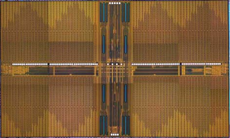
Elpida Memory announced that it had completed the development of 50nm process DDR3 SDRAM. The new DRAM product features the lowest power consumption in the industry, the 2.5Gbps speed and the 1.2V voltage at the industry's smallest chip size.
The new 50nm process DDR3 SDRAM was developed using the 193nm (ArF) immersion lithography technology and copper interconnect technology and has a chip size of less than 40mm². Also, the new SDRAM is an eco-friendly. It operates not only at the DDR3-standard 1.5V supply voltage but even at lower voltages of 1.35V and 1.2V and contributes to low-power operation of high-density memory systems such as servers and data centers.
Features of the new 50nm process DDR3 SDRAM:
- Data rate: 800Mbps, 1066Mbps, 1333Mbps, 1600Mbps, 1866Mbps, 2133Mbps and 2500Mbps
- Operating voltage: 1.2V, 1.35V, 1.5V
- Low electric current: A maximum 50% reduction (IDD4) compared to 70nm process DRAM
Mass production of the new 50nm process DDR3 SDRAM is scheduled to begin in the January-March 2009 quarter. Elpida is also aggressively developing 50nm process products for high-end digital consumer electronic products and Mobile RAM.
Source: Elpida Memory
Write a comment below. No registration needed!
|
|