Akita Elpida Memory Develops Thinnest MCP With 20 Stacked Dies
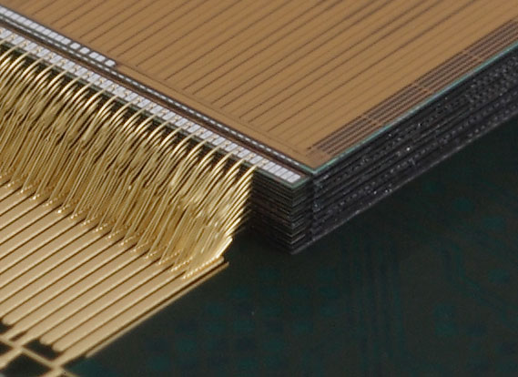
Akita Elpida Memory announced the development of a 1.4-mm thick Multi Chip Package with 20 stacked dies, making it the world's thinnest.
Its operations beginning in October of last year, Akita Elpida is a new company established in July, 2006 by Elpida Memory, with a business scope focusing on semiconductor back-end processes. Akita Elpida is currently applying its high-level technical strengths and manufacturing know-how it has developed as a member of the Hitachi group, as it currently focuses on developing and manufacturing cutting-edge, highly value-added packages known as MCPs and Package-on-Packages (PoPs), centering on products with 2 or 3 stacked dies.
Akita Elpida's technical skills which lead to the development of the world's thinnest package are introduced in the following process sequence:
- Grinding technology to achieve 30 µm thick chips
- Handling technology for 30 µm thick wafers
- Technology for picking up and die-attaching 30 µm thick chips
- 40 µm low loop wire bonding technology
- Overhang wire bonding technology
- Technology for injecting resin into narrow gap
Akita Elpida, plans from now on to put this package technology to work to establish high-yield and low-cost manufacturing technology for multi-chip stacked packages such as existing 5- and 7-die multi-chip stacked packages.
Source: Elpida Memory
Write a comment below. No registration needed!
|
|