Samsung Announces First 40nm 32Gb NAND Flash With Charge Trap
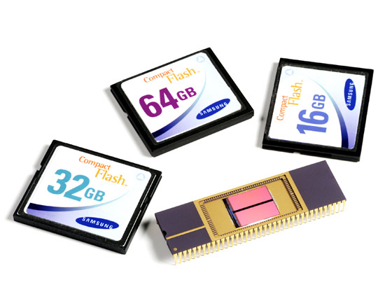
Samsung Electronics Co., Ltd. today announced that it has developed the first 40-nanometer memory device. The new 32 Gigabit NAND flash device is the first memory to incorporate a Charge Trap Flash (CTF) architecture, a new approach to further increase manufacturing efficiency while improving performance. The 32Gb NAND flash memory can be used in memory cards with densities of up to 64GB.
According to the source, the new CTF-based NAND flash memory increases the reliability of the memory by sharply reducing inter-cell noise levels. Its simple structure also enables higher scalability which will eventually improve manufacturing process technology from 40 nm to 30 and even 20nm.
In each 32Gb device, the control gate in the CTF is only 20% as large as a conventional control gate in a typical floating gate structure. With CTF, there is no floating gate. Instead, the data is temporarily placed in a holding chamber of the non-conductive layer of the flash memory composed of silicon nitride (SiN). This results in a higher level of reliability and better control of the storage current.
The CTF design is enabled through the use of a TANOS structure comprised of tantalum (metal), aluminum oxide (high k material), nitride, oxide and silicon. The use of a TANOS structure marks the first application of a metal layer coupled with a high k material to the NAND device.
The TANOS CTF architecture, which serves as the foundation of the 40nm 32Gb CTF NAND flash announced today, was developed after extensive research of the Samsung Semiconductor R&D department. Samsung first revealed the TANOS structure through a paper at the 2003 International Electron Devices Meeting (IEDM).
The new 32Gb CTF memory was announced at the sixth annual Samsung press conference in Seoul.
Source: Samsung Electronics Co., Ltd.
Write a comment below. No registration needed!