On the clock rates of GeForce 7800 GTX GPU
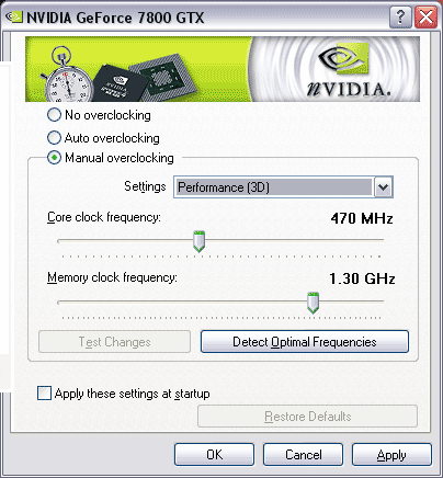
Straight away, here´s a screenshot of drivers control panel with a nominal 3D clock rate of Gainward´s G70-based card:
As you can see, it´s all correct and the clock rates are 470/1300 MHz, as promised. However when we tested the reference card we noticed that RivaTuner tool (by A. Nikolaychuk aka Unwinder) indicated some other clock rate that was about 40MHz higher than nominal (430MHz reference + 40MHz = 470MHz). The matter is that at that time Rivatuner determined the maximal clocking value.
Together with the developer of this utility we started to investigate the matter testing the card with ±5MHz steps and dumping register reports. We found out there were THREE clock rates at once! Now there´s information in the Web that NVIDIA privately mentions more clock rate values as the GPU itself consists of multiple unit, each of which is able to work at its own clock rate. This makes it obscure which clock rate should be considered primary and be placed on package boxes, etc. It would be logical to consider rasterizer and pixel pipeline clock rate primary, but now it turns out this unit is also divisible, as there´s at least ROP and Shader unit.
In other words, this is still not clear, but since both of these sub-units work at the same clock rate, it can be taken as the base. Exactly this value is declared 430MHz of the reference card and 470MHz of this Gainward´s product.
But then what was that 40MHz higher clock rate? Well, it´s geometry unit clock rate. And since it consists of vertex pipelines, we can say they are operating at 470MHz. Right after the G70 announcement ASUS informed that its card will work at this very rate. We haven´t examined this product yet, but can assume that company´s marketing team decided to name 470MHz of the geometry unit as primary. Thus we guess the SmartDoctor utility will indicate this clock rate like the RivaTuner 15.6. Again, these are just our assumptions and, perhaps, Asus, like Gainward, will change the base clock rate as well.
So, let´s describe the primary (base) clock rate again. Of all said above we see that there are THREE units with possibly different clock rates: ROP, Shader Unit and Vertex Unit. Alexey Nikolaychuk has already differentiaed these in his new Rivatuner 15.7 that is to be released soon:
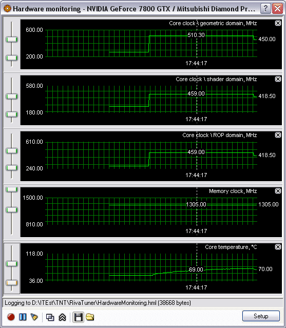
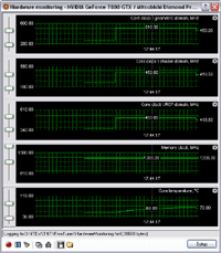
Also note however that in 2D mode all three units work at the same 275MHz. When 3D is enabled (you will see it in a video included into our next article), we can see the clock raise to different extents: the geometry unit clocked strictly to 470MHz of BIOS + 40MHz = 510MHz, while other two began working at 459MHz, not the 470MHz.
The investigation indicated that ROP and Shader Unit clock rates are changed by the drivers synchronously with the geometry unit and it´s impossible at the moment to change them separately. Second, the increment of this is 27MHz! The card features 27MHz quartz clock and the drivers select the clock rate by multipliers. In our case its like this:
27MHz * 16 / 1 = 432 MHz
These are the very 432MHz (declated as 430MHz) of the reference card. And the further overclocking can give us only 459MHz, 486MHz, 513MHz, etc. Thus 470MHz is not possible for these two GPU units today! Again, this is drivers´ feature, therefore the situation might change with the newer versions.
So, the drivers just selects clock rate which is the closest to the value set in its control panel. 470MHz is closer to 459 than to 486, that´s why we can see 459MHz indicated by the monitoring utility. So the real clock rates are 459/1300 MHz and 510MHz of the geometry unit.
As you remember, since GeForce FX series, the high-end card can work in THREE modes: 3D High Power, 3D Low Power and 2D. The average power mode haven´t been presented in NVIDIA´s drivers, so it was unaccessible unless you used RivaTuner.
These three modes are still present today. The 3D Low Power is enabled after you quit a 3D application.
As we can see, the transition to 275MHz of the 2D mode is not performed at once, but after 3-5 seconds of 418MHz (3D Low Power) mode. Note that the drivers use other multipliers for this clock rate:
27MHz * 31 / 2 = 418.5 ÌÃö
This exactly indicates that potentially the drivers can use different multipliers, so the aforementioned 27MHz increments might change in the future.
To draw a bottom line, we have found out that there are 3 GPU units with potentially different clock rate, but the drivers keep them in batch with the only exclusion of flexible geometry unit multipliers that allow us to change geometry unit clock rate within the range of the half of the fixed ROP/Shader Units increment (27MHz), given the ROP/Shader Units clock rate doesn´t change.
We´ve also found out that Vertex Unit clock rate is strictly higher by the same 40MHz set by BIOS.
Our work is not finished yet, as according NVIDIA, there are more then 3 units with different clock rates in the new GPU.
But this actually means one thing: from now on you can´t say "this GPU works at this clock rate", or at least you should also mention which clock rate this is: ROP or the Shader Unit, since they affect performance most.
Write a comment below. No registration needed!