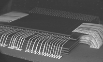
Toshiba develops 1.4mm MCP package with 9 component layers
Toshiba developed the new MCP package 1.4mm high that can include 9 component layers. To create it, the company used its latest technologies, includin the 70nm-high memory chips (the smallest for MCP). The previous company´s solutions were 85nm high, so the new package can hold up to 6 chip layers and 3 dividing layers. Therefore in terms of layer number per MCP increase, the company achieved 50% gain.
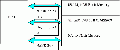
Toshiba´s new package can hold any memory chips, including SRAM, SDRAM, Pseudo SRAM, NOR, NAND, etc., up to 776Mbit. Besides space saving, the new package optimizes CPU<->MCP interconnection thanks to the triple-data bus system (dedicated bus for each memory type). The highest bus bandwidth is provided for SDRAM and NOR, the average speed is meant for SRAM and NOR, and a separate bus is used for NAND.
Package specs:
- 6 memory chips, 3 dividing layers
- Supports SRAM (8Mb x 1), SDRAM (128Mb x 1), NOR Flash Memory (128Mb x 3), NAND Flash Memory (256Mb x 1)
- Sized 11x14x1.4mm
- 1.8V voltage
- 255 pins (FBGA)
- Triple-data bus system
Write a comment below. No registration needed!
|
|


