Details about Intel´s 3D transistor
Last Wednesday we reported that Intel developed a 3D tri-gate transistor design. New details were to be announced at International Solid-State Devices and Materials. So, here they are.
3D tri-gate Intel transistor has a cubical structure, resembling an embossed surface with vertical sides.
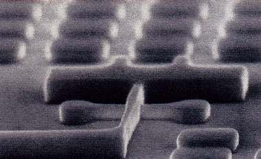
It enables to send electric signals both along the transistor "roof", and "walls". This greatly enlarges signal passage space, similar to splitting a single road to a wider highway, but does not require additional space.
The company showed slides, illustrating the difference from a usual 2D FinFET...
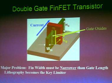
The traditional element structure is lithographically limited. The new 3D transistor...
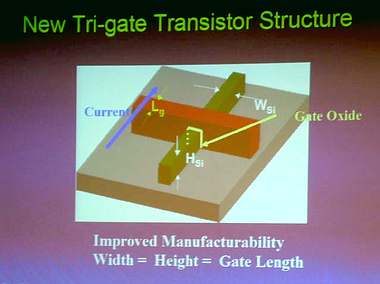
...works more effectively, conducting 20% more drive current than a traditional planar design with a similar gate size.
Tri-gate is based on ultrathin layer of fully depleted silicon, providing lower leakage current. This enables faster transistor turn-on/off at significantly low power consumption. Another feature is raised source and drain, providing lower resistance and enabling transistor to require less power. The new design is compatible with a high-penetrability K-gate dielectric, being developed now, providing even lower leakage current.
Intel plans to release a special tech brief to describe the performance, power consumption, leakage current of new transistors as well as new design advancements. The detailed info on 3D tri-gate transistors will be posted at
www.intel.com/research/silicon.
Photos provided by PC Watch
Write a comment below. No registration needed!


