 |
||
|
||
| ||
|
||
|
||
| ||
[an error occurred while processing this directive]
Reference Information on RADEON R[V]4XX Graphics Cards Reference Information on RADEON R[V]5XX Graphics Cards Reference Information on RADEON R[V]6XX Graphics Cards Reference Information on RADEON R[V]7XX Graphics Cards R[V]7XX GPU Specifications
Specifications of R[V]7XX-based reference cards
Details: RV770, RADEON HD 4800 Series
RADEON HD 4870 Specifications
RADEON HD 4850 Specifications
RV770 ArchitectureWhen engineers designed the new GPU, their main objective was to increase its efficiency. The task was to achieve two-fold advantage in theoretical performance versus the prev-gen GPU – RV670. In the light of the latest tendencies, it was also very important to improve GPU features in the field of non-graphics computing. Besides, it was the first time when they tried GDDR5 memory and crossed the psychological barrier of one teraflop (computing performance). NVIDIA almost reached it with its GT200. The RV770 architecture combines several solutions from the previous R6xx architecture, but it has been significantly overhauled to improve its performance and efficiency. Let's have a look at the diagram of the new GPU: 
We can see a lot of changes in the RV770 architecture in comparison with the architecture used in the R600 and RV670, both quantitative and qualitative. Many bottlenecks were removed. But let's be consistent and examine the changes one by one... The main part of the RV770 chip consists of ten SIMD cores, each one containing 16 blocks of superscalar streaming processors, 160 all in all. The superscalar nature of these processors hasn't changed since RV670. So we can say that the GPU contains 160*5=800 scalar 32-bit streaming processors. The same units are used for 64-bit computations of double precision, only the computing rate drops. The chip also includes other modifications: TMUs were modified and their number was increased, faster ROPs, cardinally changed memory/cache architecture, support for GDDR5, and other changes to raise the speed of executing geometry shaders and parallel non-graphics computations. 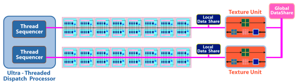
As we have already mentioned, each of ten SIMD cores contains 16 superscalar streaming processors (or 80 scalar ones), 16 KB of local memory to store data, and an individual dispatch processor. Besides, unlike R6x0 and RV670, TMUs are tied to a SIMD. Each of them has four dedicated texture units and L1 texture cache. The SIMD cores can exchange data using 16 KB of global memory. As we can see, the power of texture units in the new GPU is scaled together with the number of shader processors. ALUs relate to TMUs as 4:1. 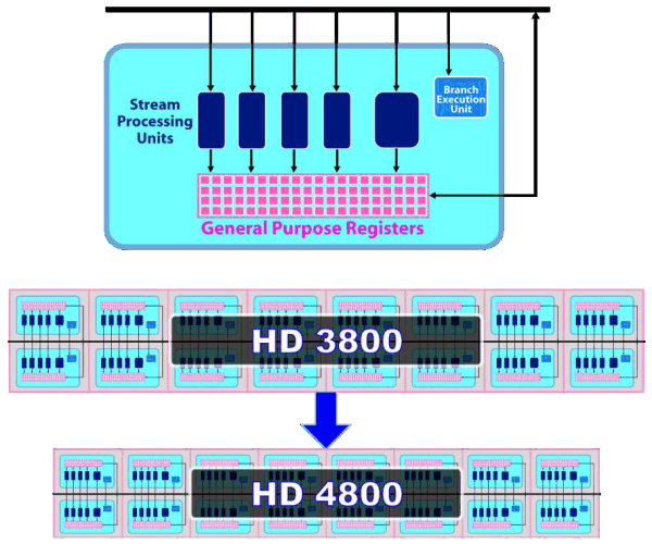
Streaming processors haven't changed since RV670, but their density has been increased (the picture is a scaled version). So the number of streaming processors was increased to 800 with the same fabrication process. More aggressive clock gating is used to raise energy efficiency. It allows to disable logic units to reduce power consumption. Besides, the superscalar design of streaming processors allowed AMD to implement support for double precision computing (FP64) using the same units in a more effective, easier way. As a result, RV770 offers much higher performance here, even though GT200 features special SPs for FP64 computations. The theoretical peak reaches 240 gigaflops. 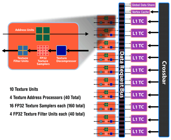
Texture units have been significantly overhauled. Now they are tied to SIMD, and their efficiency is improved. Engineers removed the dedicated TMU pool, available in previous generations. So the current solution is similar to what NVIDIA did with TMUs, included into SIMD cores. It's now impossible to fetch data without filtering, which could be done with vertex data. Texels and vertices are fetched by the same units in the new GPU, just like in the G8x and higher. On the other hand, each of 40 texture units in the RV770 is a tad weaker than each of 16 units in RV670. But there are more of them, and they operate at higher frequencies, so they should provide significant texturing performance gains. On the whole, one can expect up to 2.5-fold performance gains for bilinear filtering of 32-bit textures, and 1.25-fold gains for 64-bit textures. Other peculiarities – doubled T-Cache bandwidth versus RV670, and fetching up to 160 texture samples (Fetch4/Gather4) per cycle, which must also raise performance. 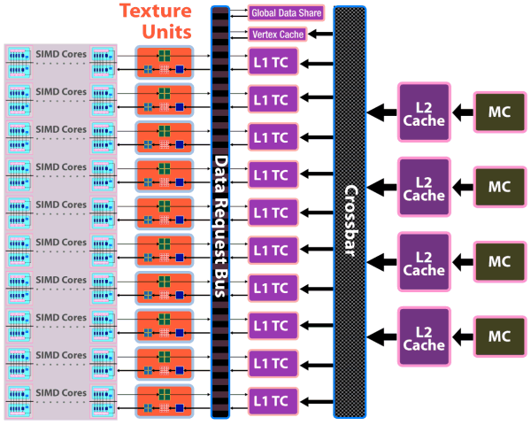
The chip uses a new design of caching units: separate vertex cache, L2 cache is tied to four 64-bit memory channels, L1 caches store unique data for each SIMD to raise caching efficiency. Bandwidth has grown as well: up to 480 GB/sec for L1 T-Cache, up to 384 GB/sec between L1 and L2 Caches. The above mentioned changes in texture units and caches make texturing performance of the RV770 twice as effective as in competing GPUs from NVIDIA (both G92 and GT200). Let's examine the ROP diagram: 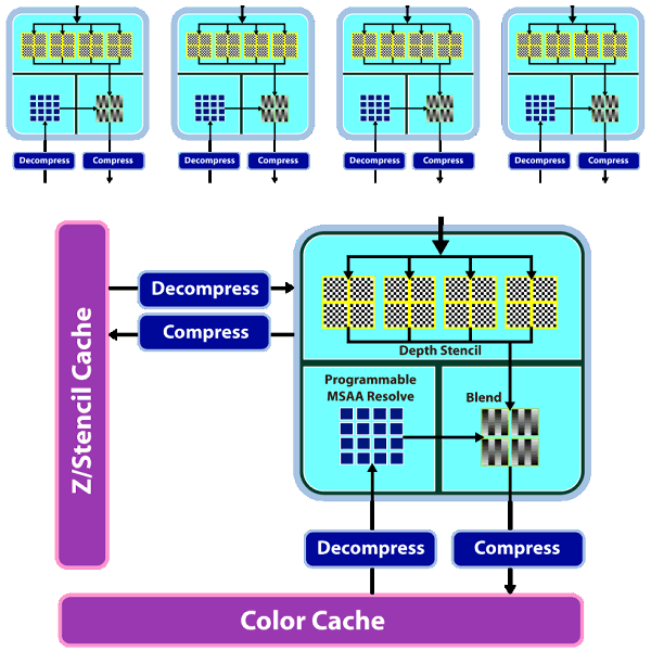
As we can see, there are not many qualitative changes in ROPs. Even though the number of ROPs hasn't changed since RV670, they can now process twice as many pixels per cycle in most cases, which is especially important for MSAA. Now algorithms of MSAA 2x and 4x come almost for "free", at least from the point of view of ROP operation. Here is a comparative table of the speed at which pixels are written into a frame buffer in various modes: 
ROPs are twice as efficient almost in all modes, except for the simplest one – 32-bit color without MSAA. We should also note Custom Filter Anti-Aliasing (CFAA). The previous generation of AMD GPUs offered special antialiasing filters called Custom Filter Anti-Aliasing. We analyzed this method in previous articles. The most interesting antialiasing feature in AMD chips is edge detect used in CFAA 12x and 24x. This method offers the highest quality. It uses the shader power of RV670 and RV770 to process images, which already went through MSAA. The method consists in detecting polygon edges (special filter) and applying additional filtering to these image areas. It does not require additional video memory as in case of MSAA 4x and 8x, and it works together with adaptive antialiasing. RV770 features minor improvements to accelerate all methods. One of them is a special fast link between ROP and shader processors. We have information that RV770 does not use shader processors for MSAA, unlike R6xx and RV670. Standard MSAA algorithms use ROPs, only programmable CFAA uses shader resources. 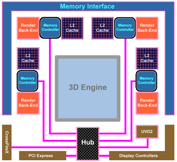
Another major change in the GPU is the upgrade from the widely advertized ring bus, which however was a failure, to the architecture with a central hub. Memory controllers in the RV770 are on the periphery of the chip, near the main traffic consumers. And the hub distributes data flows between the above mentioned units, as well as PCI Express, CrossFireX, UVD2, output controllers. According to the company's estimates, the new design of the memory interface significantly raised efficiency of bandwidth utilization. Besides, the controller supports new GDDR5 memory modules, operating at the frequency effectively quadrupled to 3.6-4 GHz and higher, which gives us memory bandwidth of up to 120 GB/sec with an inexpensive 256-bit interface. Prime costs are important, because a 512-bit bus is required to raise GDDR3 bandwidth, which leads to a larger GPU and its package. Cards themselves become bigger and more complex, consuming more power. Upgrading to GDDR5 allows to raise performance by 2-3 times and keep GPUs smaller, consuming less power. AMD was taking an active part in the development of GDDR5 standard together with all major memory manufacturers (Hynix, Qimonda, and Samsung) and JEDEC. This memory type took three years to develop, from the very beginning to the final specs. AMD spent even more time on this project. GDDR5 memory is planned to operate at up to 7 GHz of effective (quadrupled) frequency. The first 0.5-2 Gbit chips supporting 1.5 V (unlike 2.0 V for GDDR3) can operate at up to 1000*4=4.0 GHz. To conclude the architectural part of the review, we should publish the GPU diagram that shows GPU surface areas occupied by various units. As we can see, most part of the GPU is occupied by 800 streaming processors, a significant part of the chip is taken by texture processors and various controllers. To all appearances, the remaining part is occupied by ROPs, L2 Caches, and other auxiliary logic units. 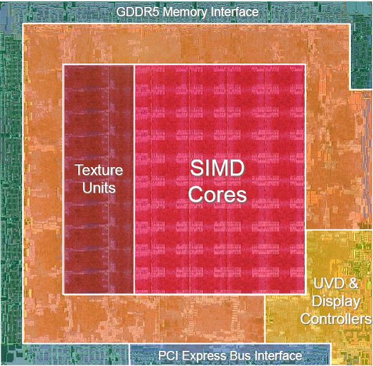
Just like in the GT200, the RV770 offers higher execution efficiency of geometry shaders, to be more exact – higher speed of generating vertex data. The GPU supports four times as many geometry execution threads, lots of generated vertices can be stored in the GPU. The tessellator is also said to be modified. Now it's compatible with DirectX 10 and 10.1 (whatever it means), it also supports instancing. We shall have a look at the speed of executing geometry shaders in our synthetic tests in the next part of the article. The tessellator was described in the baseline article about the R600. Drawing a bottom line, we can say that the GPU can be called RV-"correction-of-mistakes"-770. All apparent bugs in the RV670 design were fixed. The number of ROPs hasn't changed, but they are twice as fast now, doing twice as much work per cycle in most cases. As a result, algorithms of MSAA 2x and 4x for RADEON HD 4800 come almost free of ROP charge, although memory bandwidth limitations may still reduce performance. These are not all changes. TMUs were also overhauled. The dedicated TMU pool was removed. The new solution includes TMUs into each of ten SIMD cores. Another major change is the upgrade of the ring bus to the hub architecture. It's interesting to note that almost all changes bring the RV770 GPU closer to what we see in NVIDIA solutions. It seems that ATI(AMD) have learned to admit their mistakes and fix them. Good of them. All we have to do now is to benchmark the new solutions. Non-graphical computationsNo wonder that both major GPU manufacturers have recently paid special attention to non-graphical computations on graphics cards. GPU computing has gradually found its way to scientific fields and regular software, used in everyday tasks. For example, there have already been released (or will be soon) updated versions of Adobe Photoshop, Adobe Premier, Cyberlink PowerDirector. Hardware acceleration of physical computations in games is already used by NVIDIA PhysX. In order to raise performance and flexibility of parallel non-graphical computations, several changes have been introduced into RV770:

AMD publishes the following relative performance graph (RV670 and RV770) in synthetic computing tasks. The average performance difference between two generations amounts to 2.5-3 times (which matches the increased number of streaming processors). But the maximum performance gain was reached in the FFT algorithm – performance difference reached seven times here. AES encryption has been accelerated almost four times. That's the effect of architectural changes. ATI AvivoRV770 has a built-in Unified Video Decoder of the second generation (UVD 2). It decodes video data in all popular formats: H.264, VC-1, and MPEG2. This unit can decode two full-scale (1080p) streams simultaneously. It offers better video post processing features – there have been added scaling DVD video to HD resolutions and dynamic contrast adjustment. 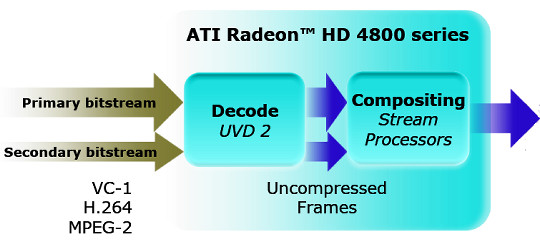
Other important innovations include support for 24- and 30-bit displays (up to 2560x1600 via DisplayPort). HDMI output is also supported through DVI-2-HDMI adapters, up to 1920x1080. The new audio controller is a real improvement. Now it supports uncompressed stereo stream with the sampling rate of 48 kHz or eight-channel (7.1) stream in AC3 format with the bitrate up to 6.144 Mbps. It's a new surge of interest to hardware-assisted video encoding and re-encoding from one format into another. AMD calls it Accelerated Video Transcoding (AVT). It supports H.264 and MPEG2. The company claims that 1080p video is re-encoded faster than 30 FPS – that is faster than in real time, on the fly. In fact, the speed of GPU-assisted encoding is similar to that of NVIDIA solutions – it takes Core 2 Duo E8500 almost ten hours to re-encode one-hour 1080p video clip, while RADEON HD 4800 copes with it for 32 minutes. That is the new GPUs are 20 times as fast as dual-core processors. To crown it all, Cyberlink PowerDirector 7 will be released soon, which will support GPU-assisted encoding. PowerPlay power managementDynamic power management technology, ATI PowerPlay, came from GPUs for notebooks. But it was improved. A special control circuit in a GPU monitors its load and determines an optimal operating mode by controlling clock rates of a GPU, memory, voltages, and other parameters, optimizing power consumption and heat release. For example, voltages and frequencies (as well as fan speed) will be minimized under low 2D load. Under average 3D load all parameters will be set to medium. And when the GPU works at full capacity, voltages and clock rates will be set to maximum. A special microcontroller is integrated into the GPU for power management. It constantly monitors temperatures and bus activity, both internal and PCI Express. The driver controls everything – clock rates of the GPU and memory, voltages, fan speed. It can also disable idle GPU units. Owing to the updated power management technology and other modifications, the new GPU is twice as efficient in terms of performance per Watt. Details: RV730, RADEON HD 4600 Series
RADEON HD 4670 Specifications
RADEON HD 4650 Specifications
Details: RV710, RADEON HD 4500 Series
RADEON HD 4550 Specifications
RV730/RV710 ArchitectureIn fact, all theoretical data about the new AMD architecture is published in our baseline article devoted to RV770. Low-End GPUs, to be reviewed today, have only quantitative differences from RV770 (with little nuances). This architecture scales well both ways, we can see it in these Low-End solutions. Here are the diagrams of RV730 and RV710: 

We can see that RV730 differs from RV760 in the number of various execution units: ALU, ROP, TMU. Everything else is the same. RV710 has more differences, not only quantitative (fewer ALUs, ROPs, and TMUs), but also one qualitative -- L1 Cache is used for both vertex and pixel data, unlike separate caches in more expensive solutions. The key quantitative changes: the number of shader processors in RV730 is reduced to 64 (320 ALU), 16 in RV710 (80 ALU), the number of texture units is reduced to 32 and 8 correspondingly. But this time the cheap solutions have different numbers of ROPs -- 8 and 4 for RV730 and RV710. By the way, RV730/RV710 and RV770 contain different numbers of SIMD cores and streaming processors inside each core (eight ALUs instead of sixteen ones). All these changes are introduced to reduce the number of transistors and surface area of the die, which will naturally slow this chip down relative to the fastest GPU in this series. You can read about the other architectural features of RV7xx in our baseline review, the link to this article is published above. Besides, the cheap solutions use 128-bit (RV730) and 64-bit (RV710) buses instead of a 256-bit one. Everything else published in that review holds true for these solutions as well. The most important change in the new GPUs is a different ratio between the number of TMUs and ALUs in comparison with RV770. Although each SIMD core has four dedicated texture units, the number of ALUs inside SIMD is different, and the ratio between ALUs and TMUs is 2:1 now instead of 4:1. That is the number of texture units in RV730 was decreased insignificantly versus RV770 (from 40 to 32), while the number of ALUs was decreased from 800 to 320. It looks like AMD has made another step away from the R6xx/RV6xx architecture. Each of 32 and 8 texture units in RV730 and RV710 is a tad weaker than in RV6xx, but there are more of them, so they should yield some gain in texture fetch performance. Let's talk about the new memory type used in HD 4600/HD 4500 cards. It's for the first time that AMD uses DDR3 memory chips (do not confuse them with GDDR3!) in mainstream graphics cards. Even though it offers the same performance level as GDDR3 (at the same frequencies, of course), prices for DDR3 memory are expected to come down to the level of DDR2 chips in the nearest future. So graphics cards manufacturers will have an opportunity to install larger volumes of relatively fast video memory. ATI AvivoJust like the top GPU in this series, RV730 and RV710 have a built-in Unified Video Decoder of the second generation (UVD 2). It appeared in Radeon HD 3000 cards, and then it was adapted to HD 4000 without significant changes. UVD2 decodes video data in all popular formats: H.264, VC-1, and MPEG-2. This video processor was modified in the new HD 4000 solutions to be able to decode two full-size (1080p) video streams simultaneously to support some Blu-ray features. Besides, improved post processing features were added, such as scaling DVD video to HD resolutions and dynamic contrast adjustment. Improved Scaling ATI Avivo in Radeon HD 4000 products includes high-quality video scaling from low (for example, DVD) into HD resolutions (720p, 1080p). Thus, ATI Avivo HD can scale standard DVDs (720x480 or 720x576) to HD devices (1920x1080 or 1920x1200) with better quality than the usual software scaling in players. That's what AMD demonstrates in its presentations: 
We can see that the left part of the image is sharper than the right part, both vertically and horizontally. We'll try to analyze this issue in more detail in our future tests of performance and quality of hardware-assisted video decoding. Dynamic Contrast Adjustment Contrast has a strong impact on how we perceive visual data. Low-contrast images usually look pale and less sharp, when small details are hard to distinguish in some areas of the image. Most players allow to adjust contrast. But these settings do not change from scene to scene, although optimal settings of contrast will be different for various scenes. ATI Avivo HD allows to change video contrast dynamically. Special post processing algorithms automatically adjust contrast, constantly adapting to changing video parameters. It improves the way a human eye perceives video, providing more details and higher sharpness (see the image on the left): 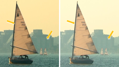
Details: R700, RADEON HD 4800 X2 Series
RADEON HD 4870 X2 Specifications
RADEON HD 4850 X2 Specifications
ArchitectureLet's proceed to the boring part. We have nothing to add to what we have already published. RV770 hasn't been modified. Its architecture has been described in detail in the corresponding article. Let's dwell on some peculiarities of using multiple GPUs. In the times of HD 3870 X2 we mentioned that it did not support PCI Express 2.0, even though it was one of the key innovations in the RV670. That graphics card used a special PCI Express bridge (PLX PEX 8547) to connect its two GPUs, which supported 48 lanes of PCI-E 1.1. Back then AMD had planned to integrate this PCI Express bridge into future GPUs. Let's see what has been done in HD 4870 X2. The dispatcher is still installed between two GPUs to link them. To all appearances, this chip is from the so-called second generation of PCI Express bridges manufactured by the same PLX Technology, one of the leading manufacturers of PCI Express solutions for Input/Output systems and internal wiring. As the company has no products with a similar designation (see the photo in the next part of the article), this chip might have been manufactured specially for AMD. Its characteristics resemble PEX8647, which is proved by documentation published on the official web site. The second generation of PLX bridges was announced in the beginning of 2008. It's notable for relatively low latencies (140 ns), very low power consumption (about 3.8 W), and flexible configuration. This bridge provides three PCI-E ports compliant with Specs 2.0, 16 lanes each. Sixteen PCI-E lanes are dedicated to connect to each RV770, and just as many lanes are used to exchange data between a motherboard and a graphics card. The new model differs from PEX8547 (used in HD 3870 X2) in PCI Express 2.0 support, smaller package dimensions, and better power saving (the old solution consumed about 5 W). Let's analyze the diagram of links between the GPUs and a motherboard, provided by AMD. It compares HD 3870 X2 and HD 4870 X2: 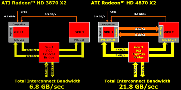
You'll notice right away theoretical values of general bandwidth, which differ three-fold in these generations: 21.8 GB/s versus 6.8 GB/s (that's the total in all directions, of course). Well, let's find out where this difference comes from. Firstly, it's the effect of the bridge supporting PCI Express 2.0 instead of 1.1. This feature provided a greater part of bandwidth, doubling it in all directions. External link with the bandwidth of 0.9 GB/s hasn't changed. But the secret sideport, mentioned in early diagrams of RV770, turned out to be an additional port (similar to a 16-channel PCI-E 2.0, judging by its bandwidth) solely for data exchange between the GPUs, by-passing the bridge and a motherboard. Will it provide any serious advantages? Unlikely. Just because the main part of limitations has to do not with bandwidth between GPUs, but with peculiarities of used algorithms. Well, theoretically, data exchange (off-screen render buffers) must go faster, but it's hardly the main limitation of AFR performance. It would have been interesting to compare performance of a single HD 4870 X2 and two HD 4870 cards (with 1 GB of video memory and operating at the same frequencies) in CrossFire, in order to evaluate contribution of this interchip channel. But in its documents, AMD prefers to compare the speed of the new card with 512 MB modifications of HD 4870 in CrossFire, obtaining performance advantages, as the latter cards suffer from insufficient video memory in heavy modes. HD 4870 X2 itself operates as a dual-GPU system, but ATI CrossFireX technology allows to connect two such cards on a single motherboard. According to AMD, such a system provides high efficiency of multi-GPU rendering in high resolutions with antialiasing and anisotropic filtering, performance gains from each GPU reach 75-80%. Reference Information on RADEON R[V]4XX Graphics Cards Reference Information on RADEON R[V]5XX Graphics Cards Reference Information on RADEON R[V]6XX Graphics Cards Reference Information on RADEON R[V]7XX Graphics Cards Write a comment below. No registration needed!
|
Platform · Video · Multimedia · Mobile · Other || About us & Privacy policy · Twitter · Facebook Copyright © Byrds Research & Publishing, Ltd., 1997–2011. All rights reserved. | |||||||||||||||||||||||||||||||||||||||||||||||||||||||||||||||||||||||||||||||||||||||||||||||||||||||||||||||||||||||||||||||||||||||||||||||||||||||||||||||||||||||||||||||||||||||||||||||


